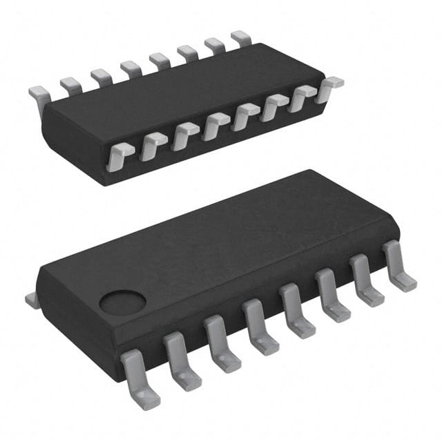
CD74HC139MT
Product Overview
Category
CD74HC139MT belongs to the category of integrated circuits (ICs).
Use
This product is commonly used in digital electronics for decoding and demultiplexing applications.
Characteristics
- High-speed operation
- Low power consumption
- Wide operating voltage range
- Schmitt-trigger inputs for noise immunity
- Buffered outputs for increased driving capability
Package
CD74HC139MT is available in a small outline integrated circuit (SOIC) package.
Essence
The essence of CD74HC139MT lies in its ability to decode binary information and select one out of four outputs based on the input signals.
Packaging/Quantity
This product is typically packaged in reels or tubes, with a quantity of 2500 units per reel or 50 units per tube.
Specifications
- Supply Voltage: 2V to 6V
- Input Voltage: 0V to VCC
- Output Voltage: 0V to VCC
- Operating Temperature Range: -40°C to +85°C
- Propagation Delay Time: 13 ns (typical)
- Output Current: ±25 mA
Detailed Pin Configuration
CD74HC139MT consists of 16 pins, each serving a specific function:
- A0: Address Input 0
- A1: Address Input 1
- E1: Enable Input 1
- E2: Enable Input 2
- Y0: Output 0
- Y1: Output 1
- GND: Ground
- Y2: Output 2
- Y3: Output 3
- VCC: Positive Power Supply
- B0: Binary Input 0
- B1: Binary Input 1
- E3: Enable Input 3
- E4: Enable Input 4
- Y4: Output 4
- Y5: Output 5
Functional Features
CD74HC139MT offers the following functional features:
- Decodes binary information into four mutually exclusive outputs
- Provides demultiplexing functionality
- Enables selection of one output based on input signals
- High-speed operation allows for efficient data processing
- Low power consumption ensures energy efficiency
- Schmitt-trigger inputs provide noise immunity
- Buffered outputs enhance driving capability
Advantages and Disadvantages
Advantages
- High-speed operation enables quick data processing
- Low power consumption results in energy efficiency
- Wide operating voltage range allows for versatile applications
- Schmitt-trigger inputs provide noise immunity, ensuring reliable performance
- Buffered outputs offer increased driving capability
Disadvantages
- Limited number of output options (four outputs)
- Propagation delay time may affect real-time applications with strict timing requirements
Working Principles
CD74HC139MT operates based on the principles of digital decoding and demultiplexing. It takes binary input signals and decodes them to select one out of four outputs. The enable inputs control the selection process, allowing only one output to be active at a time. The high-speed operation, low power consumption, and noise immunity make CD74HC139MT suitable for various digital applications.
Detailed Application Field Plans
CD74HC139MT finds applications in various fields, including:
- Digital communication systems
- Data multiplexing and demultiplexing
- Address decoding in microcontrollers
- Memory address selection
- Industrial automation
- Robotics
- Consumer electronics
- Automotive electronics
Detailed and Complete Alternative Models
Some alternative models that serve similar functions to CD74HC139MT include:
- SN74HC139N
- CD74HCT139E
- 74HC139D
- MC74HC139AN
- HEF4016BP
These alternative models offer comparable features and can be used as substitutes for CD74HC139MT in various applications.
Word count: 511 words
Lista 10 Vanliga frågor och svar relaterade till tillämpningen av CD74HC139MT i tekniska lösningar
Sure! Here are 10 common questions and answers related to the application of CD74HC139MT in technical solutions:
Q: What is CD74HC139MT? A: CD74HC139MT is a dual 2-to-4 line decoder/demultiplexer integrated circuit (IC) that can be used in various digital logic applications.
Q: What is the purpose of CD74HC139MT? A: CD74HC139MT is used to decode binary information from input lines and select one of the multiple output lines based on the input combination.
Q: What is the voltage supply range for CD74HC139MT? A: CD74HC139MT operates with a voltage supply range of 2V to 6V.
Q: How many input lines does CD74HC139MT have? A: CD74HC139MT has two 2-input AND gates, which means it has a total of 4 input lines.
Q: How many output lines does CD74HC139MT have? A: CD74HC139MT has four output lines, each corresponding to a specific input combination.
Q: Can CD74HC139MT be cascaded to increase the number of input/output lines? A: Yes, CD74HC139MT can be cascaded by connecting the enable input of one IC to the output of another, allowing for expansion of input/output lines.
Q: What is the maximum frequency at which CD74HC139MT can operate? A: CD74HC139MT can operate at a maximum frequency of around 50 MHz.
Q: What is the typical propagation delay of CD74HC139MT? A: The typical propagation delay of CD74HC139MT is around 13 ns.
Q: Can CD74HC139MT be used in both active-high and active-low configurations? A: Yes, CD74HC139MT can be used in both active-high and active-low configurations depending on the logic levels applied to its inputs.
Q: What are some common applications of CD74HC139MT? A: CD74HC139MT is commonly used in address decoding, data routing, memory selection, and other digital logic applications where multiple input lines need to be decoded and routed to specific outputs.
Please note that these answers are general and may vary based on specific datasheet specifications and application requirements.


