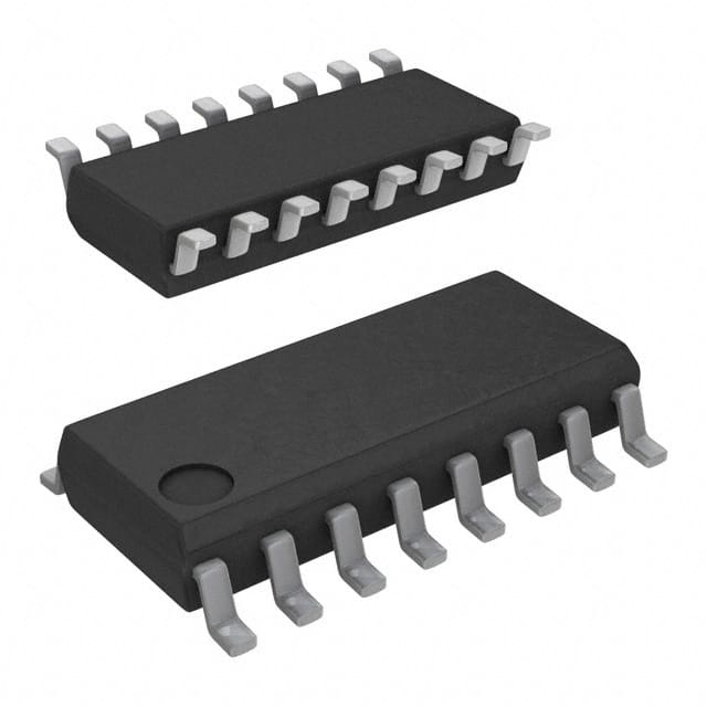
CD74HCT367MT
Product Overview
Category
CD74HCT367MT belongs to the category of integrated circuits (ICs).
Use
This product is commonly used in digital electronics and computer systems.
Characteristics
- High-speed operation
- Low power consumption
- Wide operating voltage range
- Compatibility with TTL inputs
- Schmitt-trigger action on all inputs
Package
CD74HCT367MT is available in a small outline integrated circuit (SOIC) package.
Essence
The essence of CD74HCT367MT lies in its ability to provide high-speed, low-power, and reliable digital signal processing.
Packaging/Quantity
This product is typically packaged in reels or tubes, with quantities varying based on customer requirements.
Specifications
- Supply Voltage: 2V to 6V
- Input Voltage: 0V to VCC
- Output Voltage: 0V to VCC
- Operating Temperature Range: -40°C to +85°C
- Number of Pins: 16
Detailed Pin Configuration
- OE (Output Enable)
- A1 (Input A1)
- B1 (Input B1)
- Y1 (Output Y1)
- GND (Ground)
- Y2 (Output Y2)
- B2 (Input B2)
- A2 (Input A2)
- OE (Output Enable)
- Y3 (Output Y3)
- GND (Ground)
- Y4 (Output Y4)
- B3 (Input B3)
- A3 (Input A3)
- OE (Output Enable)
- VCC (Supply Voltage)
Functional Features
- Quad 3-state outputs
- Buffered inputs
- Output capability: 10 LSTTL loads
- Outputs directly interface to CMOS, NMOS, and TTL
- High noise immunity
Advantages and Disadvantages
Advantages
- High-speed operation allows for efficient digital signal processing.
- Low power consumption helps in reducing energy usage.
- Wide operating voltage range provides flexibility in various applications.
- Compatibility with TTL inputs enables easy integration into existing systems.
- Schmitt-trigger action on all inputs ensures reliable signal processing.
Disadvantages
- Limited output capability may restrict its use in certain high-load applications.
- The small outline integrated circuit (SOIC) package may require specialized equipment for soldering and handling.
Working Principles
CD74HCT367MT operates based on the principles of digital logic. It takes input signals, processes them using internal circuitry, and produces corresponding output signals. The quad 3-state outputs allow for multiple output configurations, providing flexibility in signal routing.
Detailed Application Field Plans
CD74HCT367MT finds applications in various fields, including: 1. Microcontrollers 2. Data communication systems 3. Industrial automation 4. Automotive electronics 5. Consumer electronics
In microcontrollers, this IC can be used for address decoding and bus interfacing. In data communication systems, it aids in signal routing and protocol conversion. In industrial automation, it facilitates control signal generation and sensor interfacing. In automotive electronics, it contributes to engine management and vehicle diagnostics. In consumer electronics, it supports signal processing and interface control.
Detailed and Complete Alternative Models
Some alternative models that offer similar functionality to CD74HCT367MT include: 1. SN74HCT367N by Texas Instruments 2. MC74HCT367AN by ON Semiconductor 3. 74HCT367D by NXP Semiconductors 4. CD54HCT367F3A by Texas Instruments 5. DM74HCT367WM by Fairchild Semiconductor
These alternative models can be considered based on specific requirements and availability.
Word count: 532 words
Lista 10 Vanliga frågor och svar relaterade till tillämpningen av CD74HCT367MT i tekniska lösningar
Sure! Here are 10 common questions and answers related to the application of CD74HCT367MT in technical solutions:
Q: What is CD74HCT367MT? A: CD74HCT367MT is a high-speed hex buffer/driver with 3-state outputs, commonly used in digital logic circuits.
Q: What is the operating voltage range for CD74HCT367MT? A: CD74HCT367MT operates within a voltage range of 4.5V to 5.5V.
Q: What is the maximum output current that CD74HCT367MT can handle? A: CD74HCT367MT can handle a maximum output current of 6mA.
Q: Can CD74HCT367MT be used as a level shifter? A: Yes, CD74HCT367MT can be used as a level shifter to convert signals between different voltage levels.
Q: How many inputs and outputs does CD74HCT367MT have? A: CD74HCT367MT has six inputs and six 3-state outputs.
Q: What is the propagation delay of CD74HCT367MT? A: The typical propagation delay of CD74HCT367MT is around 9ns.
Q: Can CD74HCT367MT drive capacitive loads directly? A: No, it is recommended to use a series resistor when driving capacitive loads to prevent excessive current flow.
Q: Is CD74HCT367MT suitable for high-frequency applications? A: CD74HCT367MT is not specifically designed for high-frequency applications but can still be used in moderate-speed digital systems.
Q: Can CD74HCT367MT be used in bidirectional applications? A: No, CD74HCT367MT is a unidirectional buffer/driver and cannot be used for bidirectional communication.
Q: What are some typical applications of CD74HCT367MT? A: CD74HCT367MT is commonly used in address decoding, bus driving, and general-purpose digital logic circuits.
Please note that these answers are general and may vary depending on specific design requirements and datasheet specifications.


