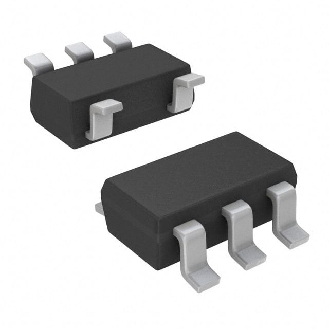
CLVC1G125MDCKREP
Product Overview
- Category: Integrated Circuit
- Use: Logic Level Shifter
- Characteristics: Single Gate, Non-Inverting
- Package: SC-70-5
- Essence: Logic Level Translation
- Packaging/Quantity: Tape and Reel, 3000 pieces per reel
Specifications
- Supply Voltage Range: 1.65V to 5.5V
- High-Level Input Voltage (VIH): 2.3V to VCC + 0.5V
- Low-Level Input Voltage (VIL): -0.5V to 0.8V
- High-Level Output Voltage (VOH): VCC - 0.4V
- Low-Level Output Voltage (VOL): 0.4V
- Maximum Propagation Delay Time: 3.9ns
- Maximum Quiescent Current: 10μA
Detailed Pin Configuration
The CLVC1G125MDCKREP has a total of 5 pins:
- GND: Ground pin
- A: Input pin for logic level shifting
- OE: Output Enable pin
- Y: Output pin for logic level shifted signal
- VCC: Power supply pin
Functional Features
- Logic level translation from low voltage to high voltage or vice versa
- Non-inverting operation preserves the input signal polarity
- Wide supply voltage range allows compatibility with various systems
- Fast propagation delay ensures quick signal transmission
- Low quiescent current minimizes power consumption
Advantages and Disadvantages
Advantages: - Compact SC-70-5 package saves board space - Wide supply voltage range enhances versatility - Non-inverting operation maintains signal integrity - Fast propagation delay enables high-speed applications
Disadvantages: - Limited number of gates in a single package - Not suitable for bidirectional level shifting
Working Principles
The CLVC1G125MDCKREP is a logic level shifter that allows translation between different voltage levels. It operates as a non-inverting buffer, meaning the output signal follows the input signal's logic state. The device utilizes a single gate to perform the level shifting function.
The input signal is connected to pin A, and the output signal is obtained from pin Y. The OE pin controls the output enable/disable functionality. When OE is low, the output is enabled, and the logic level translation occurs. Conversely, when OE is high, the output is disabled, and the output signal remains in a high-impedance state.
The device operates within a wide supply voltage range of 1.65V to 5.5V, allowing compatibility with various systems. It features a fast propagation delay of 3.9ns, ensuring quick signal transmission. Additionally, the CLVC1G125MDCKREP consumes low quiescent current, making it suitable for power-sensitive applications.
Detailed Application Field Plans
The CLVC1G125MDCKREP can be used in various applications that require logic level translation. Some potential application fields include:
- Microcontrollers: Enable communication between microcontrollers operating at different voltage levels.
- Sensor Interfaces: Facilitate connection between sensors and microcontrollers with varying voltage requirements.
- Communication Systems: Bridge the gap between different voltage domains in communication interfaces.
- Battery-Powered Devices: Efficiently interface low-power devices with higher voltage systems.
- Industrial Automation: Enable compatibility between different logic families used in automation systems.
Detailed and Complete Alternative Models
- SN74LVC1G125DBVR: Single Gate Non-Inverting Buffer, SOT-23-5 package, 3000 pieces per reel.
- NC7SZ125P5X: Single Gate Non-Inverting Buffer, SC-70-5 package, 3000 pieces per reel.
- TC7SZ125FU: Single Gate Non-Inverting Buffer, SOT-353 package, 3000 pieces per reel.
These alternative models offer similar functionality and characteristics to the CLVC1G125MDCKREP, providing options for different package preferences or availability.
Word count: 470 words
Lista 10 Vanliga frågor och svar relaterade till tillämpningen av CLVC1G125MDCKREP i tekniska lösningar
Sure! Here are 10 common questions and answers related to the application of CLVC1G125MDCKREP in technical solutions:
Q1: What is CLVC1G125MDCKREP? A1: CLVC1G125MDCKREP is a specific type of logic gate buffer/driver integrated circuit (IC) that provides voltage level shifting and signal buffering capabilities.
Q2: What is the purpose of using CLVC1G125MDCKREP in technical solutions? A2: CLVC1G125MDCKREP is commonly used to interface between different voltage domains, ensuring proper signal levels and preventing damage to sensitive components.
Q3: What voltage levels can CLVC1G125MDCKREP support? A3: CLVC1G125MDCKREP can support voltage levels ranging from 1.65V to 5.5V, making it suitable for various applications.
Q4: How many input/output channels does CLVC1G125MDCKREP have? A4: CLVC1G125MDCKREP has a single input channel and a single output channel.
Q5: What is the maximum data rate supported by CLVC1G125MDCKREP? A5: CLVC1G125MDCKREP can support data rates up to 500 Mbps, making it suitable for high-speed digital communication.
Q6: Can CLVC1G125MDCKREP be used bidirectionally? A6: No, CLVC1G125MDCKREP is unidirectional and can only be used for one-way signal transmission.
Q7: Is CLVC1G125MDCKREP compatible with different logic families? A7: Yes, CLVC1G125MDCKREP is compatible with various logic families such as CMOS, TTL, and LVCMOS.
Q8: What is the power supply voltage range for CLVC1G125MDCKREP? A8: The power supply voltage range for CLVC1G125MDCKREP is typically between 1.65V and 5.5V.
Q9: Can CLVC1G125MDCKREP handle high output currents? A9: Yes, CLVC1G125MDCKREP has a high output drive capability, allowing it to handle relatively high output currents.
Q10: Are there any specific application examples where CLVC1G125MDCKREP is commonly used? A10: Yes, CLVC1G125MDCKREP is often used in applications such as level shifting between different voltage domains, signal buffering in communication interfaces, and voltage translation in mixed-signal systems.
Please note that the answers provided here are general and may vary depending on the specific requirements and datasheet of CLVC1G125MDCKREP.


