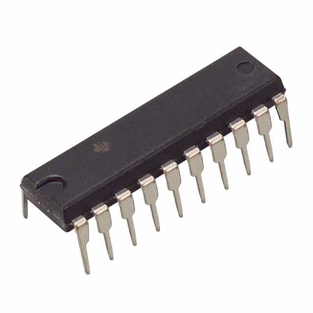
SN74AHC541N
Product Overview
- Category: Integrated Circuit (IC)
- Use: Buffer/Line Driver
- Characteristics: High-Speed, Non-Inverting, Octal Buffer/Line Driver
- Package: PDIP (Plastic Dual In-Line Package)
- Essence: A versatile buffer/line driver IC designed to provide high-speed signal amplification and transmission capabilities.
- Packaging/Quantity: Available in tubes or reels, with varying quantities depending on the supplier.
Specifications
- Supply Voltage Range: 2 V to 5.5 V
- Input Voltage Range: 0 V to VCC
- Output Voltage Range: 0 V to VCC
- Maximum Operating Frequency: 50 MHz
- Number of Buffers/Drivers: 8
- Output Current: ±8 mA
- Propagation Delay Time: 6 ns (typical)
Detailed Pin Configuration
The SN74AHC541N has a total of 20 pins, which are arranged as follows:
+---\/---+
   OE1 |1      20| VCC
   A1  |2      19| A2
   Y1  |3      18| Y2
   A3  |4      17| A4
   Y3  |5      16| Y4
   A5  |6      15| A6
   Y5  |7      14| Y6
   A7  |8      13| A8
   GND |9      12| OE2
   Y7  |10     11| Y8
       +--------+
Functional Features
- Non-Inverting Buffer/Line Driver: The SN74AHC541N amplifies and transmits input signals without inverting their polarity.
- High-Speed Operation: With a maximum operating frequency of 50 MHz, it is suitable for applications requiring fast signal transmission.
- Octal Configuration: The IC consists of eight independent buffer/drivers, allowing simultaneous amplification and transmission of multiple signals.
- Wide Voltage Range: It can operate with a supply voltage ranging from 2 V to 5.5 V, making it compatible with various digital systems.
Advantages and Disadvantages
Advantages
- High-speed operation enables efficient signal transmission.
- Non-inverting nature preserves the original signal polarity.
- Octal configuration provides versatility in handling multiple signals.
- Wide voltage range allows compatibility with different systems.
Disadvantages
- Limited output current may not be suitable for driving heavy loads.
- Propagation delay time of 6 ns may introduce slight delays in signal transmission.
Working Principles
The SN74AHC541N operates by receiving input signals on its A1-A8 pins. These signals are then amplified and transmitted through the corresponding Y1-Y8 pins. The OE1 and OE2 pins control the enable/disable function of the buffer/drivers. When the enable pins are active (low), the IC amplifies and transmits the input signals. Conversely, when the enable pins are inactive (high), the IC goes into a high-impedance state, effectively disconnecting the input and output lines.
Detailed Application Field Plans
The SN74AHC541N finds applications in various fields, including:
- Digital Communication Systems: Used for signal buffering and line driving in data transmission circuits.
- Microcontroller Interfacing: Enables communication between microcontrollers and external devices by providing signal amplification and level shifting capabilities.
- Industrial Automation: Facilitates signal transmission in control systems, motor drives, and sensor interfaces.
- Automotive Electronics: Utilized in automotive control modules, infotainment systems, and communication networks for reliable signal amplification and transmission.
- Consumer Electronics: Integrated into audio/video equipment, gaming consoles, and home automation systems to enhance signal integrity during data transfer.
Detailed and Complete Alternative Models
- SN74AHC540N: Similar to SN74AHC541N but with an inverting buffer/driver configuration.
- SN74LVC541A: Low-voltage version of the SN74AHC541N, designed for operation at 1.65 V to 3.6 V supply voltage range.
- MC74HCT541AN: A TTL-compatible alternative with Schmitt-trigger inputs, suitable for mixed logic systems.
These alternative models offer similar functionality and can be considered as replacements based on specific application requirements.
Word count: 531 words
Lista 10 Vanliga frågor och svar relaterade till tillämpningen av SN74AHC541N i tekniska lösningar
Sure! Here are 10 common questions and answers related to the application of SN74AHC541N in technical solutions:
Q: What is SN74AHC541N? A: SN74AHC541N is a type of integrated circuit (IC) commonly used as a buffer or line driver in digital systems.
Q: What is the purpose of using SN74AHC541N in a technical solution? A: SN74AHC541N is used to amplify or buffer digital signals, ensuring proper signal integrity and driving capability.
Q: What voltage levels does SN74AHC541N support? A: SN74AHC541N supports voltage levels between 2V and 5.5V, making it compatible with a wide range of digital systems.
Q: Can SN74AHC541N be used for bidirectional communication? A: Yes, SN74AHC541N can be used for bidirectional communication by enabling its output enable (OE) pin.
Q: How many channels does SN74AHC541N have? A: SN74AHC541N has 8 channels, allowing it to handle multiple input/output signals simultaneously.
Q: What is the maximum current that SN74AHC541N can drive? A: SN74AHC541N can drive up to 8mA of current per channel, making it suitable for most digital applications.
Q: Is SN74AHC541N tolerant to electrostatic discharge (ESD)? A: Yes, SN74AHC541N has built-in ESD protection, which helps safeguard it against damage from static electricity.
Q: Can SN74AHC541N operate at high speeds? A: Yes, SN74AHC541N is designed to operate at high-speed digital signals, with a typical propagation delay of around 6ns.
Q: Can SN74AHC541N be cascaded or daisy-chained with other ICs? A: Yes, SN74AHC541N can be cascaded or daisy-chained with other ICs to expand the number of input/output channels.
Q: What are some common applications of SN74AHC541N? A: SN74AHC541N is commonly used in microcontrollers, data communication systems, memory interfaces, and general-purpose digital circuits.
Please note that these answers are general and may vary depending on specific design considerations and requirements.


