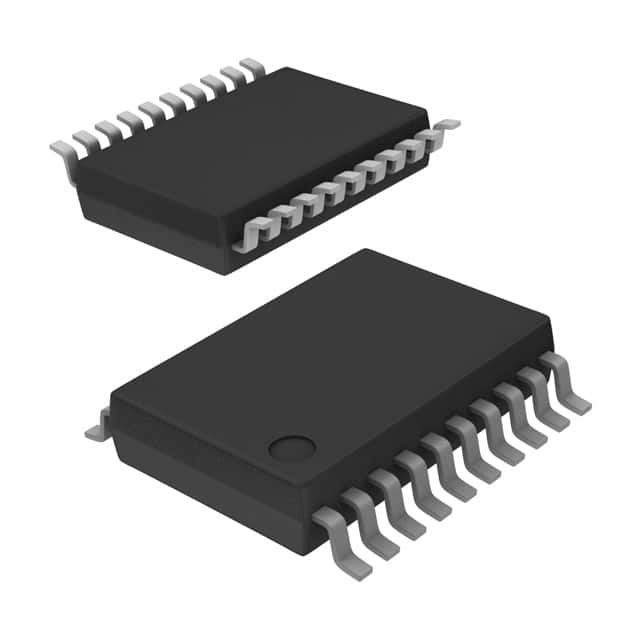
SN74AHCT541DBRE4
Product Overview
- Category: Integrated Circuit
- Use: Buffer/Line Driver
- Characteristics: High-Speed, Low-Power, Octal Buffer/Line Driver
- Package: SSOP (Shrink Small Outline Package)
- Essence: A high-performance buffer/line driver designed for use in various digital applications.
- Packaging/Quantity: Tape and Reel, 2500 units per reel
Specifications
- Supply Voltage Range: 4.5V to 5.5V
- Input Voltage Range: 0V to VCC
- Output Voltage Range: 0V to VCC
- Operating Temperature Range: -40°C to +85°C
- Output Drive Capability: ±24mA at 3.3V
- Propagation Delay: 6ns (typical)
- Input Capacitance: 3pF (typical)
Detailed Pin Configuration
The SN74AHCT541DBRE4 has a total of 20 pins, which are arranged as follows:
__    __
   1 |* 1  20 *| VCC
   2 | 2  19 | A1
   3 | 3  18 | A2
   4 | 4  17 | A3
   5 | 5  16 | A4
   6 | 6  15 | A5
   7 | 7  14 | A6
   8 | 8  13 | A7
 GND | 9  12 | OE#
  B1 |10  11 | B2
      ‾‾    ‾‾
Functional Features
- Octal buffer/line driver with 3-state outputs
- Non-inverting outputs
- High-speed operation with minimal power consumption
- Compatible with TTL and CMOS logic levels
- Schmitt-trigger inputs for noise immunity
- Output current limiting and thermal shutdown protection
Advantages and Disadvantages
Advantages: - High-speed operation allows for efficient data transfer - Low-power consumption helps in reducing overall system energy requirements - 3-state outputs provide flexibility in controlling bus lines - Wide supply voltage range enables compatibility with various systems - Schmitt-trigger inputs ensure reliable operation in noisy environments
Disadvantages: - Limited output drive capability compared to some other buffer/line driver ICs - Relatively higher propagation delay compared to certain specialized ICs
Working Principles
The SN74AHCT541DBRE4 is designed to buffer and drive digital signals. It takes input signals from the A1-A7 pins and provides non-inverted outputs on the B1-B2 pins. The OE# pin controls the output enable/disable function, allowing the device to be put into a high-impedance state when not actively driving the bus lines.
The IC operates by amplifying and shaping the input signals using internal circuitry. It utilizes CMOS technology, which provides high-speed operation while consuming low power. The Schmitt-trigger inputs help in maintaining signal integrity by providing noise immunity.
Detailed Application Field Plans
The SN74AHCT541DBRE4 can be used in various applications, including but not limited to:
- Data communication systems: Used to buffer and drive signals between different components of a communication system, such as microcontrollers, memory devices, and peripheral interfaces.
- Industrial automation: Enables signal buffering and driving in control systems, PLCs (Programmable Logic Controllers), and motor control circuits.
- Automotive electronics: Suitable for use in automotive systems, such as ECU (Engine Control Unit), infotainment systems, and sensor interfaces.
- Consumer electronics: Used in devices like smartphones, tablets, and gaming consoles for signal buffering and driving between different components.
Detailed and Complete Alternative Models
- SN74AHCT541-Q1: Automotive-grade version with enhanced ESD (Electrostatic Discharge) protection.
- SN74AHCT540: Octal buffer/line driver with inverting outputs.
- SN74AHCT244: Octal buffer/line driver with 3-state outputs and higher output drive capability.
- SN74LVC541A: Octal buffer/line driver with lower voltage operation (2.7V to 3.6V) and faster propagation delay.
These alternative models provide similar functionality but may have differences in specifications, package types, or additional features based on specific application requirements.
Word count: 550 words
Lista 10 Vanliga frågor och svar relaterade till tillämpningen av SN74AHCT541DBRE4 i tekniska lösningar
Sure! Here are 10 common questions and answers related to the application of SN74AHCT541DBRE4 in technical solutions:
Question: What is SN74AHCT541DBRE4?
- Answer: SN74AHCT541DBRE4 is a type of octal buffer/line driver with 3-state outputs, commonly used in digital systems.Question: What is the operating voltage range for SN74AHCT541DBRE4?
- Answer: The operating voltage range for SN74AHCT541DBRE4 is from 4.5V to 5.5V.Question: How many inputs and outputs does SN74AHCT541DBRE4 have?
- Answer: SN74AHCT541DBRE4 has 8 inputs and 8 outputs.Question: Can SN74AHCT541DBRE4 be used for level shifting?
- Answer: Yes, SN74AHCT541DBRE4 can be used for level shifting as it supports both TTL and CMOS logic levels.Question: What is the maximum output current that SN74AHCT541DBRE4 can drive?
- Answer: SN74AHCT541DBRE4 can drive up to 8mA of output current per channel.Question: Is SN74AHCT541DBRE4 suitable for bidirectional communication?
- Answer: No, SN74AHCT541DBRE4 is not bidirectional. It is designed for unidirectional data transfer.Question: Can SN74AHCT541DBRE4 handle high-speed signals?
- Answer: Yes, SN74AHCT541DBRE4 is capable of handling high-speed signals with a typical propagation delay of 9ns.Question: Does SN74AHCT541DBRE4 have internal pull-up or pull-down resistors?
- Answer: No, SN74AHCT541DBRE4 does not have internal pull-up or pull-down resistors. External resistors may be required.Question: Can SN74AHCT541DBRE4 be used in automotive applications?
- Answer: Yes, SN74AHCT541DBRE4 is qualified for automotive applications and meets the AEC-Q100 standard.Question: What is the package type of SN74AHCT541DBRE4?
- Answer: SN74AHCT541DBRE4 comes in a small-outline integrated circuit (SOIC) package with 20 pins.
Please note that these answers are general and may vary depending on specific application requirements.


