

SN74ALVC04DGVR
Product Overview
- Category: Integrated Circuit (IC)
- Use: Logic Gate
- Characteristics: High-speed, low-power, hex inverter
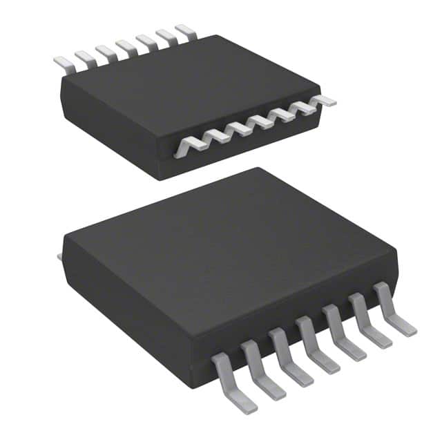
- Package: VSSOP-8
- Essence: Digital logic gate
- Packaging/Quantity: Tape and Reel, 2500 units per reel
Specifications
- Supply Voltage Range: 1.65V to 3.6V
- Input Voltage Range: 0V to VCC
- Output Voltage Range: 0V to VCC
- Operating Temperature Range: -40°C to +85°C
- Propagation Delay Time: 2.5ns (typical)
- Output Drive Capability: ±24mA
- Input Capacitance: 3pF (typical)
Detailed Pin Configuration
The SN74ALVC04DGVR has a VSSOP-8 package with the following pin configuration:
____
   A1 |    | VCC
   A2 |    | Y1
   B1 |    | Y2
   B2 |    | GND
   C1 |    | Y3
   C2 |    | Y4
   D1 |    | Y5
   D2 |    | Y6
       ----
Functional Features
- Hex inverter with high-speed operation
- Low power consumption
- Wide supply voltage range for compatibility with various systems
- High output drive capability for driving capacitive loads
- Excellent noise immunity
- Schmitt-trigger input for improved noise rejection
Advantages
- Fast switching speed allows for high-performance applications
- Low power consumption reduces energy requirements
- Wide supply voltage range enables compatibility with different systems
- High output drive capability ensures reliable signal transmission
- Noise immunity and Schmitt-trigger input enhance signal integrity
Disadvantages
- Limited number of inverters (6) in a single package
- Not suitable for applications requiring more complex logic functions
Working Principles
The SN74ALVC04DGVR is a hex inverter IC that converts input logic levels to their complementary values. It utilizes CMOS technology, which allows for high-speed operation and low power consumption. The Schmitt-trigger input ensures noise immunity by providing hysteresis and rejecting small voltage fluctuations. The output drive capability enables the IC to drive capacitive loads without compromising signal integrity.
Detailed Application Field Plans
The SN74ALVC04DGVR finds applications in various digital systems, including:
- Microprocessors and microcontrollers
- Communication systems
- Data transmission equipment
- Industrial automation
- Consumer electronics
- Automotive electronics
In these applications, the IC is used for signal inversion, level shifting, waveform generation, and other logic functions.
Detailed and Complete Alternative Models
- SN74LVC04A: Similar hex inverter with lower supply voltage range (1.65V to 5.5V)
- SN74HC04: Hex inverter with higher supply voltage range (2V to 6V) and faster propagation delay time
- SN74LV1T04: Single inverter with lower power consumption and smaller package size
These alternative models offer similar functionality but may have different specifications and characteristics.
Lista 10 Vanliga frågor och svar relaterade till tillämpningen av SN74ALVC04DGVR i tekniska lösningar
Sure! Here are 10 common questions and answers related to the application of SN74ALVC04DGVR:
Q: What is SN74ALVC04DGVR? A: SN74ALVC04DGVR is a hex inverter gate IC (integrated circuit) that provides six independent inverters in a single package.
Q: What is the voltage supply range for SN74ALVC04DGVR? A: The voltage supply range for SN74ALVC04DGVR is typically between 1.65V and 3.6V.
Q: What is the maximum output current of SN74ALVC04DGVR? A: The maximum output current of SN74ALVC04DGVR is typically around 24mA.
Q: Can SN74ALVC04DGVR be used in both digital and analog applications? A: No, SN74ALVC04DGVR is primarily designed for digital applications and may not perform optimally in analog circuits.
Q: What is the propagation delay of SN74ALVC04DGVR? A: The propagation delay of SN74ALVC04DGVR is typically around 3.8ns.
Q: Can SN74ALVC04DGVR tolerate overvoltage on its inputs? A: Yes, SN74ALVC04DGVR has built-in protection diodes that can tolerate limited overvoltage on its inputs.
Q: Is SN74ALVC04DGVR compatible with both CMOS and TTL logic levels? A: Yes, SN74ALVC04DGVR is compatible with both CMOS and TTL logic levels, making it versatile for various applications.
Q: Can SN74ALVC04DGVR drive capacitive loads directly? A: Yes, SN74ALVC04DGVR can drive small capacitive loads directly without requiring additional buffering.
Q: What is the operating temperature range for SN74ALVC04DGVR? A: The operating temperature range for SN74ALVC04DGVR is typically between -40°C and 85°C.
Q: Can SN74ALVC04DGVR be used in battery-powered applications? A: Yes, SN74ALVC04DGVR's low power consumption and wide voltage supply range make it suitable for battery-powered applications.
Please note that these answers are general and may vary depending on specific datasheet specifications and application requirements.