

SN74ALVC126DGVR
Product Overview
Category
SN74ALVC126DGVR belongs to the category of integrated circuits (ICs).
Use
It is commonly used as a quad buffer/line driver with 3-state outputs.
Characteristics
- Low voltage CMOS technology
- High-speed operation
- 3-state outputs for bus-oriented applications
- Schmitt-trigger inputs for noise immunity
- Available in various package options
Package
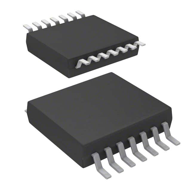
SN74ALVC126DGVR is available in a small-sized VSSOP-14 package.
Essence
The essence of SN74ALVC126DGVR lies in its ability to provide buffering and line driving functions, making it suitable for use in digital systems.
Packaging/Quantity
SN74ALVC126DGVR is typically packaged in reels or tubes, with each reel/tube containing a specific quantity of ICs.
Specifications
- Supply Voltage: 1.65V to 3.6V
- Input Voltage: 0V to VCC
- Output Voltage: 0V to VCC
- Operating Temperature Range: -40°C to +85°C
- Propagation Delay Time: 2.5ns (max)
- Output Current: ±24mA
Detailed Pin Configuration
SN74ALVC126DGVR has a total of 14 pins, which are labeled as follows:
- GND (Ground)
- A1 (Input A1)
- Y1 (Output Y1)
- A2 (Input A2)
- Y2 (Output Y2)
- G (Enable Input)
- Y3 (Output Y3)
- A3 (Input A3)
- Y4 (Output Y4)
- VCC (Supply Voltage)
- B1 (Input B1)
- B2 (Input B2)
- B3 (Input B3)
- B4 (Input B4)
Functional Features
- Quad buffer/line driver with 3-state outputs
- High-speed operation for efficient data transfer
- Schmitt-trigger inputs provide noise immunity
- Enables bus-oriented applications
Advantages and Disadvantages
Advantages
- Low voltage CMOS technology ensures low power consumption
- High-speed operation allows for quick data transmission
- 3-state outputs enable easy bus sharing
- Schmitt-trigger inputs provide noise immunity, enhancing reliability
Disadvantages
- Limited output current capacity
- Restricted operating temperature range (-40°C to +85°C)
Working Principles
SN74ALVC126DGVR operates by receiving input signals from the A1-A4 and B1-B4 pins. These signals are then buffered and amplified before being transmitted through the Y1-Y4 output pins. The G pin acts as an enable input, controlling the 3-state outputs. When G is high, the outputs are active, and when G is low, the outputs are in a high-impedance state.
Detailed Application Field Plans
SN74ALVC126DGVR finds application in various digital systems, including but not limited to: - Microcontrollers - Data communication systems - Industrial automation - Automotive electronics - Consumer electronics
Detailed and Complete Alternative Models
Some alternative models that can be considered as alternatives to SN74ALVC126DGVR include: - SN74LVC126A - SN74LVCH126 - SN74AHC126 - SN74AHCT126
These models offer similar functionality and characteristics, providing flexibility in choosing the most suitable option for specific applications.
In conclusion, SN74ALVC126DGVR is a versatile integrated circuit used for buffering and line driving purposes in digital systems. Its low voltage CMOS technology, high-speed operation, and 3-state outputs make it a reliable choice for various applications. However, it is important to consider its limitations, such as limited output current capacity and restricted operating temperature range.
Lista 10 Vanliga frågor och svar relaterade till tillämpningen av SN74ALVC126DGVR i tekniska lösningar
Sure! Here are 10 common questions and answers related to the application of SN74ALVC126DGVR:
Question: What is the SN74ALVC126DGVR?
- Answer: The SN74ALVC126DGVR is a quad buffer/line driver with 3-state outputs, commonly used in digital logic applications.Question: What is the operating voltage range of SN74ALVC126DGVR?
- Answer: The operating voltage range of SN74ALVC126DGVR is from 1.65V to 3.6V.Question: What is the maximum output current of SN74ALVC126DGVR?
- Answer: The maximum output current of SN74ALVC126DGVR is ±24mA.Question: Can SN74ALVC126DGVR be used for level shifting?
- Answer: Yes, SN74ALVC126DGVR can be used for level shifting as it supports both 3.3V and 5V logic levels.Question: What is the propagation delay of SN74ALVC126DGVR?
- Answer: The propagation delay of SN74ALVC126DGVR is typically around 3.8ns.Question: Is SN74ALVC126DGVR compatible with other logic families?
- Answer: Yes, SN74ALVC126DGVR is compatible with various logic families such as TTL, CMOS, and LVCMOS.Question: Can SN74ALVC126DGVR drive capacitive loads?
- Answer: Yes, SN74ALVC126DGVR can drive capacitive loads up to 50pF.Question: Does SN74ALVC126DGVR have built-in protection features?
- Answer: Yes, SN74ALVC126DGVR has built-in protection features like overvoltage and undervoltage lockout.Question: What is the package type of SN74ALVC126DGVR?
- Answer: SN74ALVC126DGVR comes in a small SOT-23-5 package.Question: Can SN74ALVC126DGVR be used in high-speed applications?
- Answer: Yes, SN74ALVC126DGVR can be used in high-speed applications as it has a maximum operating frequency of 400MHz.
Please note that these answers are general and may vary depending on specific application requirements. It's always recommended to refer to the datasheet and consult with technical experts for accurate information.