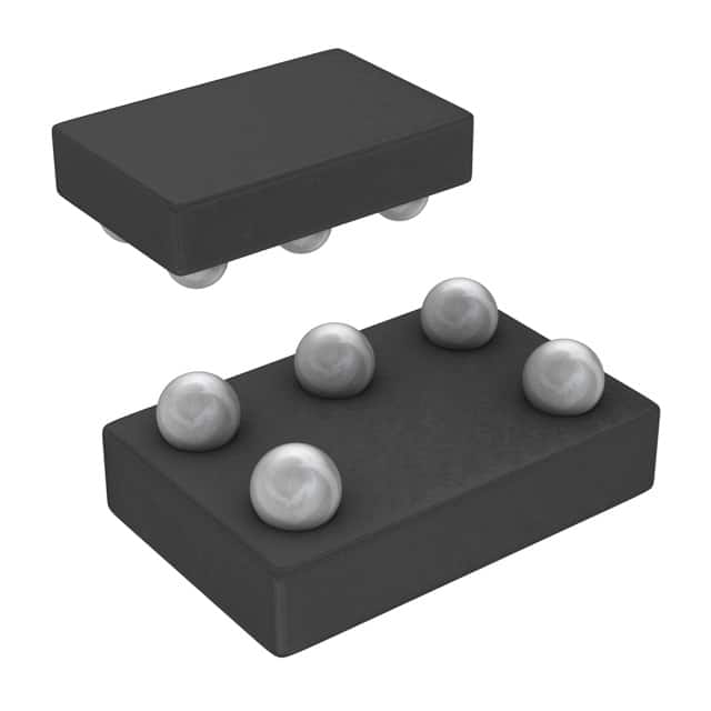
SN74AUC1G125YZAR
Product Overview
- Category: Integrated Circuit
- Use: Buffer/Driver
- Characteristics: Single Gate, Non-Inverting, Tri-State Output
- Package: SOT-23-5
- Essence: High-Speed CMOS Logic
- Packaging/Quantity: Tape and Reel, 3000 pieces per reel
Specifications
- Supply Voltage Range: 0.8V to 3.6V
- Input Voltage Range: 0V to VCC
- Output Voltage Range: 0V to VCC
- Maximum Operating Frequency: 500 MHz
- Propagation Delay: 2.9 ns (typical)
- Output Drive Capability: ±24 mA
- Operating Temperature Range: -40°C to +85°C
Detailed Pin Configuration
The SN74AUC1G125YZAR has a total of 5 pins:
- GND (Ground): Connected to the ground reference voltage.
- VCC (Supply Voltage): Connected to the positive supply voltage.
- OE (Output Enable): Controls the tri-state output buffer.
- A (Input): Accepts the input signal to be buffered.
- Y (Output): Provides the buffered output signal.
Functional Features
- Single gate buffer with non-inverting functionality.
- Tri-state output allows for high impedance when disabled.
- High-speed operation suitable for various applications.
- Wide supply voltage range enables compatibility with different systems.
- Low power consumption for energy-efficient designs.
Advantages and Disadvantages
Advantages: - Small package size saves board space. - High-speed operation supports fast data transmission. - Tri-state output provides flexibility in bus systems. - Wide supply voltage range enhances versatility.
Disadvantages: - Limited output drive capability compared to some other models. - Not suitable for high-power applications.
Working Principles
The SN74AUC1G125YZAR is a single gate buffer that amplifies and buffers the input signal. It operates using high-speed CMOS logic, which allows for fast switching times and low power consumption. The non-inverting functionality ensures that the output signal follows the input signal's logic level.
The tri-state output feature enables the device to enter a high-impedance state when the output enable (OE) pin is set to a specific logic level. This allows multiple devices to share a common bus without interfering with each other.
Detailed Application Field Plans
The SN74AUC1G125YZAR is commonly used in various applications, including:
- Communication Systems: Used as a buffer in data transmission lines to ensure signal integrity.
- Industrial Control Systems: Provides signal buffering and level shifting in control circuits.
- Automotive Electronics: Used in automotive modules for signal conditioning and level translation.
- Consumer Electronics: Integrated into portable devices for voltage level conversion and signal buffering.
- IoT Devices: Enables signal buffering and level shifting in IoT sensor nodes and communication modules.
Detailed and Complete Alternative Models
- SN74AUC1G126YZAR: Similar to SN74AUC1G125YZAR but with an additional tri-state output.
- SN74LVC1G125DBVR: Low-voltage version with similar functionality and package but operates at 1.65V to 5.5V.
- SN74HC1G125DCKR: High-speed CMOS version with similar characteristics but operates at 2V to 6V.
These alternative models offer similar functionality and can be considered based on specific application requirements.
Word count: 410 words
Lista 10 Vanliga frågor och svar relaterade till tillämpningen av SN74AUC1G125YZAR i tekniska lösningar
Sure! Here are 10 common questions and answers related to the application of SN74AUC1G125YZAR:
Q1: What is SN74AUC1G125YZAR? A1: SN74AUC1G125YZAR is a single bus buffer gate with 3-state output. It is commonly used in technical solutions for signal buffering and level shifting.
Q2: What is the operating voltage range of SN74AUC1G125YZAR? A2: The operating voltage range of SN74AUC1G125YZAR is from 0.8V to 3.6V.
Q3: What is the maximum output current of SN74AUC1G125YZAR? A3: The maximum output current of SN74AUC1G125YZAR is typically 32mA.
Q4: Can SN74AUC1G125YZAR be used for bidirectional communication? A4: No, SN74AUC1G125YZAR is a unidirectional buffer and cannot be used for bidirectional communication.
Q5: What is the propagation delay of SN74AUC1G125YZAR? A5: The propagation delay of SN74AUC1G125YZAR is typically around 2.7ns.
Q6: Can SN74AUC1G125YZAR handle high-speed signals? A6: Yes, SN74AUC1G125YZAR is designed for high-speed operation and can handle signals up to several hundred megahertz.
Q7: Is SN74AUC1G125YZAR compatible with different logic families? A7: Yes, SN74AUC1G125YZAR is compatible with various logic families such as CMOS, TTL, and LVCMOS.
Q8: Can SN74AUC1G125YZAR be used in automotive applications? A8: Yes, SN74AUC1G125YZAR is qualified for automotive applications and meets the necessary standards.
Q9: What is the package type of SN74AUC1G125YZAR? A9: SN74AUC1G125YZAR is available in a small SOT-23 package.
Q10: Are there any recommended operating conditions for SN74AUC1G125YZAR? A10: Yes, some recommended operating conditions include a supply voltage between 0.8V and 3.6V, and an ambient temperature range of -40°C to 85°C.
Please note that these answers are general and may vary depending on the specific datasheet and application requirements.


