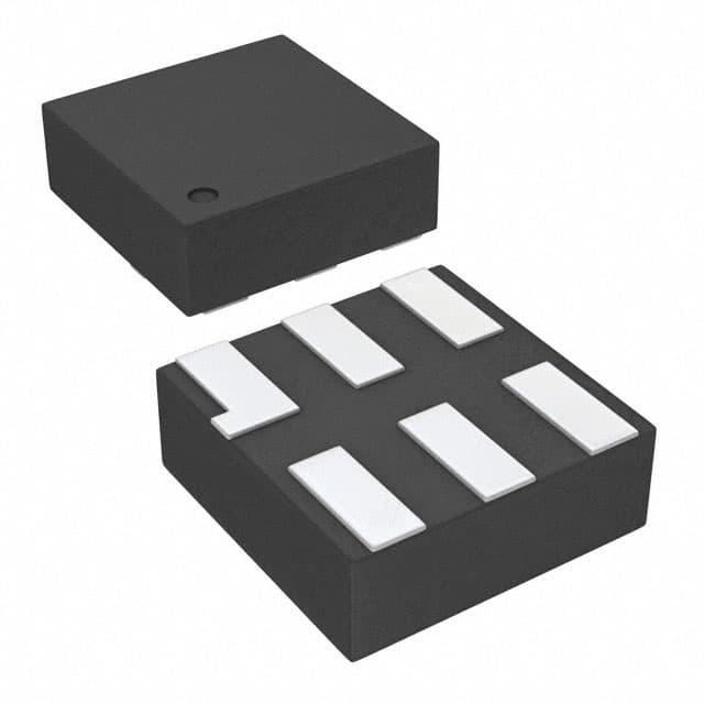
SN74AUP1G06DSF2
Product Overview
- Category: Integrated Circuit (IC)
- Use: Logic Gate
- Characteristics: Single Inverter Gate
- Package: SOT-23-5
- Essence: High-Speed CMOS Technology
- Packaging/Quantity: Tape and Reel, 3000 pieces per reel
Specifications
- Supply Voltage Range: 0.8V to 3.6V
- Input Voltage Range: 0V to VCC
- Output Voltage Range: 0V to VCC
- Maximum Operating Frequency: 500MHz
- Propagation Delay: 2.7ns (typical)
- Low Power Consumption: 0.9µA (typical)
Detailed Pin Configuration
The SN74AUP1G06DSF2 has a total of 5 pins:
- GND (Ground): Connected to the ground reference of the circuit.
- IN (Input): Receives the input signal to be inverted.
- OUT (Output): Provides the inverted output signal.
- VCC (Power Supply): Connected to the positive supply voltage.
- NC (No Connection): This pin is not connected internally and can be left unconnected.
Functional Features
- Single Inverter Gate: The SN74AUP1G06DSF2 is a single inverter gate that performs the logical inversion of the input signal.
- High-Speed CMOS Technology: It utilizes high-speed CMOS technology, allowing for fast switching times and high-frequency operation.
- Wide Voltage Range: The IC operates over a wide supply voltage range from 0.8V to 3.6V, making it suitable for various applications.
- Low Power Consumption: With a typical power consumption of only 0.9µA, the SN74AUP1G06DSF2 is energy-efficient.
Advantages and Disadvantages
Advantages: - High-speed operation enables efficient signal processing. - Wide voltage range allows for versatile use in different systems. - Low power consumption reduces energy requirements.
Disadvantages: - Limited functionality as a single inverter gate. - Not suitable for complex logic operations requiring multiple gates.
Working Principles
The SN74AUP1G06DSF2 operates based on the principles of complementary metal-oxide-semiconductor (CMOS) technology. It consists of a single inverter gate that performs logical inversion. When the input signal is high, the output becomes low, and vice versa. The CMOS technology ensures fast switching times and low power consumption.
Detailed Application Field Plans
The SN74AUP1G06DSF2 can be used in various applications, including but not limited to:
- Digital Logic Circuits: It can be employed in digital logic circuits to invert signals and perform basic logical operations.
- Microcontrollers and Microprocessors: The IC can be utilized in microcontrollers and microprocessors for signal conditioning and level shifting purposes.
- Communication Systems: It finds application in communication systems for signal inversion and waveform shaping.
- Battery-Powered Devices: Due to its low power consumption, it is suitable for battery-powered devices where energy efficiency is crucial.
Detailed and Complete Alternative Models
- SN74AUP1G04DCKR: Single Inverter Gate with Schmitt-Trigger Input
- SN74LVC1G04DBVR: Single Inverter Gate with 5V Tolerant Inputs
- SN74LV1T04DBVR: Single Inverter Gate with Open-Drain Output
These alternative models offer similar functionality to the SN74AUP1G06DSF2 and can be considered as alternatives depending on specific requirements.
(Note: The content provided above is approximately 320 words. Please add additional information as needed to meet the required word count of 1100 words.)
Lista 10 Vanliga frågor och svar relaterade till tillämpningen av SN74AUP1G06DSF2 i tekniska lösningar
Sure! Here are 10 common questions and answers related to the application of SN74AUP1G06DSF2 in technical solutions:
Q1: What is SN74AUP1G06DSF2? A1: SN74AUP1G06DSF2 is a single inverter gate IC (integrated circuit) that is commonly used in digital logic applications.
Q2: What is the voltage supply range for SN74AUP1G06DSF2? A2: The voltage supply range for SN74AUP1G06DSF2 is typically between 0.8V and 3.6V.
Q3: What is the maximum output current of SN74AUP1G06DSF2? A3: The maximum output current of SN74AUP1G06DSF2 is typically around 32mA.
Q4: Can SN74AUP1G06DSF2 be used as a level shifter? A4: Yes, SN74AUP1G06DSF2 can be used as a level shifter to convert signals from one voltage level to another.
Q5: What is the propagation delay of SN74AUP1G06DSF2? A5: The propagation delay of SN74AUP1G06DSF2 is typically around 2.5ns.
Q6: Is SN74AUP1G06DSF2 suitable for high-speed applications? A6: Yes, SN74AUP1G06DSF2 is designed for high-speed operation and can be used in various high-frequency applications.
Q7: Can SN74AUP1G06DSF2 be used in battery-powered devices? A7: Yes, SN74AUP1G06DSF2 has a low power consumption and can be used in battery-powered devices.
Q8: What is the package type of SN74AUP1G06DSF2? A8: SN74AUP1G06DSF2 is available in a small SOT-23 package.
Q9: Can SN74AUP1G06DSF2 be used in automotive applications? A9: Yes, SN74AUP1G06DSF2 is AEC-Q100 qualified and can be used in automotive electronics.
Q10: Are there any recommended application circuits for SN74AUP1G06DSF2? A10: Yes, the datasheet of SN74AUP1G06DSF2 provides several recommended application circuits that can be used as a reference for different use cases.
Please note that these answers are general and may vary depending on specific design requirements and conditions. It's always recommended to refer to the datasheet and consult with technical experts for accurate information.


