

SN74AUP1G08DPWR
Basic Information Overview
- Category: Integrated Circuit (IC)
- Use: Logic Gate
- Characteristics: Single 2-Input AND Gate
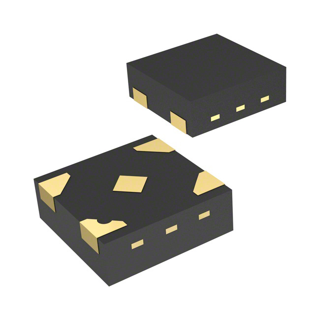
- Package: SOT-23-5
- Essence: High-Speed CMOS Technology
- Packaging/Quantity: Tape and Reel, 3000 pieces per reel
Specifications
- Supply Voltage Range: 0.8V to 3.6V
- Input Voltage Range: -0.5V to VCC + 0.5V
- Output Voltage Range: 0V to VCC
- Operating Temperature Range: -40°C to 85°C
- Propagation Delay: 2.9ns (typical) at 3.3V, 25°C
- Maximum Quiescent Current: 10μA at 3.3V, 25°C
Detailed Pin Configuration
The SN74AUP1G08DPWR has a total of 5 pins: 1. GND (Ground) 2. A (Input A) 3. B (Input B) 4. Y (Output) 5. VCC (Supply Voltage)
Functional Features
- High-Speed Operation: The SN74AUP1G08DPWR utilizes high-speed CMOS technology, allowing for fast logic gate operation.
- Low Power Consumption: With a maximum quiescent current of only 10μA, this IC is designed to minimize power consumption.
- Wide Voltage Range: The supply voltage range of 0.8V to 3.6V enables compatibility with various systems and applications.
- Small Package Size: The SOT-23-5 package offers a compact form factor, making it suitable for space-constrained designs.
Advantages and Disadvantages
Advantages: - High-speed operation allows for quick signal processing. - Low power consumption prolongs battery life in portable devices. - Wide voltage range provides flexibility in different voltage environments. - Small package size saves board space and enables compact designs.
Disadvantages: - Limited to 2-input AND gate functionality, may not be suitable for complex logic operations. - Operating temperature range of -40°C to 85°C may not be suitable for extreme temperature environments.
Working Principles
The SN74AUP1G08DPWR is a single 2-input AND gate. It operates by receiving two input signals (A and B) and producing an output signal (Y) based on the logical AND operation between the inputs. The IC utilizes high-speed CMOS technology to achieve fast switching times and low power consumption.
Detailed Application Field Plans
The SN74AUP1G08DPWR can be used in various applications, including but not limited to: - Digital Logic Systems: It can be integrated into digital circuits to perform logical AND operations, enabling complex decision-making processes. - Microcontrollers and Microprocessors: The IC can be utilized as a building block for interfacing with other components or peripherals. - Communication Systems: It can be employed in communication protocols that require logical operations, such as error detection and correction.
Detailed and Complete Alternative Models
Some alternative models that offer similar functionality to the SN74AUP1G08DPWR include: - 74HC08: A widely used 2-input AND gate IC from the 74HC series. - CD4081: A quad 2-input AND gate IC from the CD4000 series. - MC14008B: A quad 2-input AND gate IC from the MC14000 series.
These alternative models provide comparable logic gate functionality and can be considered as substitutes for the SN74AUP1G08DPWR depending on specific requirements.
Word count: 411 words
Lista 10 Vanliga frågor och svar relaterade till tillämpningen av SN74AUP1G08DPWR i tekniska lösningar
Sure! Here are 10 common questions and answers related to the application of SN74AUP1G08DPWR:
Q1: What is SN74AUP1G08DPWR? A1: SN74AUP1G08DPWR is a single 2-input AND gate IC (integrated circuit) manufactured by Texas Instruments.
Q2: What is the operating voltage range of SN74AUP1G08DPWR? A2: The operating voltage range of SN74AUP1G08DPWR is from 0.8V to 3.6V.
Q3: What is the maximum output current of SN74AUP1G08DPWR? A3: The maximum output current of SN74AUP1G08DPWR is 32mA.
Q4: Can SN74AUP1G08DPWR be used in battery-powered applications? A4: Yes, SN74AUP1G08DPWR can be used in battery-powered applications due to its low power consumption and wide operating voltage range.
Q5: What is the package type of SN74AUP1G08DPWR? A5: SN74AUP1G08DPWR comes in a small SOT-23-5 package.
Q6: Is SN74AUP1G08DPWR suitable for high-speed applications? A6: Yes, SN74AUP1G08DPWR is designed for high-speed operation, making it suitable for various digital logic applications.
Q7: Can SN74AUP1G08DPWR be used as a level shifter? A7: Yes, SN74AUP1G08DPWR can be used as a level shifter to convert signals between different voltage levels.
Q8: Does SN74AUP1G08DPWR have built-in protection features? A8: Yes, SN74AUP1G08DPWR has built-in ESD (electrostatic discharge) protection to safeguard against damage during handling and operation.
Q9: What is the typical propagation delay of SN74AUP1G08DPWR? A9: The typical propagation delay of SN74AUP1G08DPWR is around 2.5ns.
Q10: Can SN74AUP1G08DPWR be used in automotive applications? A10: Yes, SN74AUP1G08DPWR is AEC-Q100 qualified, making it suitable for use in automotive electronics.
Please note that these answers are general and may vary depending on specific application requirements.