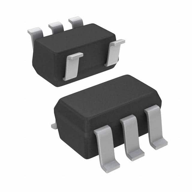
SN74AUP1G79DBVTG4
Product Overview
- Category: Integrated Circuit (IC)
- Use: Logic Gate
- Characteristics: Single Positive-Edge-Triggered D-Type Flip-Flop
- Package: SOT-23-5
- Essence: High-speed, low-power consumption flip-flop
- Packaging/Quantity: Tape and Reel, 3000 pieces per reel
Specifications
- Supply Voltage Range: 0.8V to 3.6V
- High-Speed Operation: 5.4 ns maximum propagation delay at 3.3V
- Low Power Consumption: 0.9 µA maximum ICC
- Operating Temperature Range: -40°C to +85°C
- Input/Output Compatibility: CMOS/TTL
Detailed Pin Configuration
The SN74AUP1G79DBVTG4 has a total of 5 pins:
- VCC: Positive power supply input
- GND: Ground reference
- D: Data input
- CP: Clock pulse input
- Q: Output
Functional Features
The SN74AUP1G79DBVTG4 is a single positive-edge-triggered D-type flip-flop. It operates with a supply voltage range of 0.8V to 3.6V, making it suitable for low-power applications. The high-speed operation of this flip-flop allows for quick data storage and retrieval. It is compatible with both CMOS and TTL logic levels, providing flexibility in various circuit designs.
Advantages and Disadvantages
Advantages: - Low power consumption - High-speed operation - Wide supply voltage range - Compact package size
Disadvantages: - Limited number of flip-flops in a single package - Not suitable for high-voltage applications
Working Principles
The SN74AUP1G79DBVTG4 operates as a positive-edge-triggered D-type flip-flop. When the clock pulse (CP) transitions from low to high, the data input (D) is latched and stored in the flip-flop. The stored data can then be accessed at the output (Q). This flip-flop is designed to operate with low power consumption while maintaining high-speed performance.
Detailed Application Field Plans
The SN74AUP1G79DBVTG4 is commonly used in various applications, including:
- Mobile devices: Due to its low power consumption and compact package size, this flip-flop is suitable for use in smartphones, tablets, and other portable electronic devices.
- Communication systems: The high-speed operation of the SN74AUP1G79DBVTG4 makes it ideal for use in communication systems, such as routers, switches, and network equipment.
- Industrial automation: This flip-flop can be utilized in industrial automation systems for data storage and control purposes.
- Automotive electronics: With its wide supply voltage range and compact package, the SN74AUP1G79DBVTG4 is well-suited for automotive applications, including vehicle control units and infotainment systems.
Detailed and Complete Alternative Models
- SN74AUP1G79DCKR
- SN74AUP1G79DRLR
- SN74AUP1G79DRLRG4
- SN74AUP1G79DRLRQ1
- SN74AUP1G79DRLRQ1G4
These alternative models offer similar functionality and characteristics to the SN74AUP1G79DBVTG4, providing options for different package types and quantities.
Word count: 389
Lista 10 Vanliga frågor och svar relaterade till tillämpningen av SN74AUP1G79DBVTG4 i tekniska lösningar
Sure! Here are 10 common questions and answers related to the application of SN74AUP1G79DBVTG4 in technical solutions:
Q1: What is SN74AUP1G79DBVTG4? A1: SN74AUP1G79DBVTG4 is a single positive-edge-triggered D-type flip-flop with clear, designed for 1.8-V to 3.6-V VCC operation.
Q2: What is the purpose of SN74AUP1G79DBVTG4? A2: SN74AUP1G79DBVTG4 is used to store and transfer a single bit of data in digital circuits.
Q3: What is the voltage range supported by SN74AUP1G79DBVTG4? A3: SN74AUP1G79DBVTG4 supports a voltage range of 1.8V to 3.6V.
Q4: How many inputs does SN74AUP1G79DBVTG4 have? A4: SN74AUP1G79DBVTG4 has one data input (D), one clock input (CLK), and one clear input (CLR).
Q5: What is the maximum clock frequency supported by SN74AUP1G79DBVTG4? A5: The maximum clock frequency supported by SN74AUP1G79DBVTG4 is typically around 500 MHz.
Q6: Can SN74AUP1G79DBVTG4 be used in battery-powered applications? A6: Yes, SN74AUP1G79DBVTG4 can be used in battery-powered applications as it operates within a low voltage range.
Q7: Is SN74AUP1G79DBVTG4 compatible with other logic families? A7: Yes, SN74AUP1G79DBVTG4 is compatible with other logic families such as CMOS and TTL.
Q8: What is the package type of SN74AUP1G79DBVTG4? A8: SN74AUP1G79DBVTG4 comes in a small SOT-23 package.
Q9: Can SN74AUP1G79DBVTG4 be used in high-speed applications? A9: Yes, SN74AUP1G79DBVTG4 can be used in high-speed applications due to its fast propagation delay.
Q10: Are there any special considerations when using SN74AUP1G79DBVTG4? A10: It is important to ensure that the voltage levels of the inputs and power supply are within the specified range to avoid any damage or malfunctioning of the device.


