

SN74AUP2G34YFPR
Product Overview
- Category: Integrated Circuit (IC)
- Use: Logic Gate
- Characteristics: Dual Buffer/Driver, Low Power Consumption
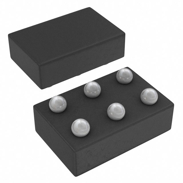
- Package: DSBGA (Dual Solder Ball Grid Array)
- Essence: This IC is designed to provide buffering and driving capabilities for digital signals in various electronic circuits.
- Packaging/Quantity: Available in tape and reel packaging, with a quantity of 3000 units per reel.
Specifications
- Supply Voltage Range: 0.8V to 3.6V
- Input Voltage Range: 0V to VCC
- Output Voltage Range: 0V to VCC
- Operating Temperature Range: -40°C to +85°C
- Propagation Delay: 1.5 ns (typical)
- Output Drive Capability: ±24 mA
Detailed Pin Configuration
The SN74AUP2G34YFPR IC has the following pin configuration:
___________
      |           |
   1 -| A         |-
   2 -| Y         |-
      |___________|
Pin Descriptions: - Pin 1 (A): Input Pin - Pin 2 (Y): Output Pin
Functional Features
- Dual Buffer/Driver: The SN74AUP2G34YFPR provides two independent buffer/driver circuits in a single package.
- Low Power Consumption: This IC is designed to operate with low power consumption, making it suitable for battery-powered devices.
- High-Speed Operation: With a propagation delay of only 1.5 ns, this IC ensures fast signal transmission.
Advantages and Disadvantages
Advantages: - Compact Size: The DSBGA package allows for a compact design, saving space on the circuit board. - Low Power Consumption: Ideal for energy-efficient applications. - High-Speed Operation: Ensures fast signal propagation.
Disadvantages: - Limited Output Drive Capability: The ±24 mA output drive capability may not be sufficient for certain high-current applications. - Temperature Limitations: The operating temperature range is limited to -40°C to +85°C, which may restrict its use in extreme environments.
Working Principles
The SN74AUP2G34YFPR operates as a buffer/driver by amplifying and shaping digital signals. It accepts an input signal at pin A and provides an amplified output signal at pin Y. The IC operates within the specified voltage range and ensures reliable signal transmission with minimal delay.
Detailed Application Field Plans
The SN74AUP2G34YFPR can be used in various electronic applications, including but not limited to: 1. Mobile Devices: Provides signal buffering and driving capabilities for display panels, touchscreens, and other mobile device components. 2. Communication Systems: Enables signal conditioning and amplification in communication systems, such as routers, modems, and wireless devices. 3. Industrial Automation: Facilitates signal transmission and interfacing in industrial automation equipment, such as PLCs (Programmable Logic Controllers) and motor control systems. 4. Automotive Electronics: Supports signal buffering and driving in automotive electronics, including infotainment systems, instrument clusters, and control modules.
Detailed and Complete Alternative Models
- SN74AUP2G34RSER: Similar to SN74AUP2G34YFPR, but available in a different package (QFN).
- SN74LVC2G34DCTR: Dual Buffer/Driver IC with similar characteristics, but operates at a higher supply voltage range (1.65V to 5.5V).
- SN74LV1T34DBVR: Single Buffer/Driver IC with comparable characteristics, suitable for applications requiring only one buffer/driver circuit.
These alternative models offer similar functionality and can be considered as substitutes for the SN74AUP2G34YFPR in different design scenarios.
Word count: 511 words
Lista 10 Vanliga frågor och svar relaterade till tillämpningen av SN74AUP2G34YFPR i tekniska lösningar
Sure! Here are 10 common questions and answers related to the application of SN74AUP2G34YFPR in technical solutions:
Q: What is SN74AUP2G34YFPR? A: SN74AUP2G34YFPR is a dual buffer gate IC (integrated circuit) that provides high-speed signal buffering in various technical applications.
Q: What is the operating voltage range of SN74AUP2G34YFPR? A: The operating voltage range of SN74AUP2G34YFPR is typically between 0.8V and 3.6V.
Q: What is the maximum output current of SN74AUP2G34YFPR? A: SN74AUP2G34YFPR can provide a maximum output current of around 24mA.
Q: Can SN74AUP2G34YFPR be used for level shifting applications? A: Yes, SN74AUP2G34YFPR can be used for level shifting as it supports both 3.3V and 1.8V logic levels.
Q: Is SN74AUP2G34YFPR suitable for high-speed data transmission? A: Yes, SN74AUP2G34YFPR is designed for high-speed operation and can handle data rates up to several hundred megahertz.
Q: Does SN74AUP2G34YFPR have built-in ESD protection? A: Yes, SN74AUP2G34YFPR has built-in ESD (electrostatic discharge) protection, which helps safeguard against electrostatic damage.
Q: Can SN74AUP2G34YFPR be used in battery-powered applications? A: Yes, SN74AUP2G34YFPR is suitable for battery-powered applications as it operates at low voltage and has low power consumption.
Q: What is the package type of SN74AUP2G34YFPR? A: SN74AUP2G34YFPR comes in a small form factor package known as DSBGA (Dual Small Ball Grid Array).
Q: Can SN74AUP2G34YFPR be used in automotive applications? A: Yes, SN74AUP2G34YFPR is automotive-grade and can be used in various automotive electronics applications.
Q: Are there any application notes or reference designs available for SN74AUP2G34YFPR? A: Yes, Texas Instruments provides application notes and reference designs that can help users understand and implement SN74AUP2G34YFPR in their technical solutions.
Please note that the answers provided here are general and may vary depending on specific requirements and use cases. It's always recommended to refer to the datasheet and consult with the manufacturer for detailed information.