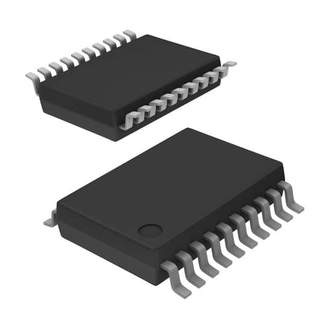
SN74BCT244DBR
Product Overview
Category
SN74BCT244DBR belongs to the category of integrated circuits (ICs).
Use
It is commonly used as a buffer/line driver in various electronic applications.
Characteristics
- High-speed CMOS technology
- 3-state outputs
- Low power consumption
- Wide operating voltage range
- Schmitt-trigger inputs for noise immunity
Package
SN74BCT244DBR is available in a standard SOIC (Small Outline Integrated Circuit) package.
Essence
The essence of SN74BCT244DBR lies in its ability to provide buffering and line driving functions, ensuring signal integrity and compatibility between different parts of an electronic circuit.
Packaging/Quantity
SN74BCT244DBR is typically sold in reels containing a quantity of 2500 units per reel.
Specifications
- Supply Voltage: 4.5V to 5.5V
- Input Voltage: 0V to VCC
- Output Voltage: 0V to VCC
- Operating Temperature Range: -40°C to +85°C
- Propagation Delay Time: 6 ns (typical)
- Output Current: ±24 mA
Detailed Pin Configuration
SN74BCT244DBR consists of 20 pins, which are assigned specific functions as follows:
- A1: Input A1
- Y1: Output Y1
- A2: Input A2
- Y2: Output Y2
- GND: Ground
- A3: Input A3
- Y3: Output Y3
- A4: Input A4
- Y4: Output Y4
- GND: Ground
- A5: Input A5
- Y5: Output Y5
- A6: Input A6
- Y6: Output Y6
- VCC: Supply Voltage
- OE: Output Enable
- Y7: Output Y7
- A7: Input A7
- Y8: Output Y8
- A8: Input A8
Functional Features
- Buffering and line driving capability
- 3-state outputs for bus-oriented applications
- Schmitt-trigger inputs for improved noise immunity
- High-speed operation suitable for time-critical applications
- Low power consumption for energy-efficient designs
Advantages and Disadvantages
Advantages
- Provides signal buffering and line driving functions
- Wide operating voltage range allows compatibility with various systems
- Schmitt-trigger inputs enhance noise immunity
- High-speed operation ensures efficient data transfer
- Low power consumption contributes to energy efficiency
Disadvantages
- Limited number of input/output channels (8 in total)
- Not suitable for applications requiring a large number of buffered signals
Working Principles
SN74BCT244DBR operates by receiving input signals on its designated input pins (A1-A8) and providing corresponding buffered output signals on the respective output pins (Y1-Y8). The output enable pin (OE) controls the activation of the output buffers. When OE is high, the outputs are enabled, allowing the transmission of signals. Conversely, when OE is low, the outputs are disabled, resulting in a high-impedance state.
Detailed Application Field Plans
SN74BCT244DBR finds application in various electronic systems, including but not limited to: - Microcontrollers and microprocessors - Memory interfaces - Data communication systems - Industrial automation - Automotive electronics - Consumer electronics
Detailed and Complete Alternative Models
Some alternative models that offer similar functionality to SN74BCT244DBR include: - SN74ACT244: Advanced CMOS version with faster switching speed - SN74HCT244: High-speed CMOS version with TTL compatibility - SN74LS244: Low-power Schottky TTL version
These alternative models can be considered based on specific requirements and design constraints.
Word count: 526 words
Lista 10 Vanliga frågor och svar relaterade till tillämpningen av SN74BCT244DBR i tekniska lösningar
Sure! Here are 10 common questions and answers related to the application of SN74BCT244DBR:
Q: What is SN74BCT244DBR? A: SN74BCT244DBR is a type of octal buffer and line driver integrated circuit (IC) that can be used in various technical solutions.
Q: What is the purpose of SN74BCT244DBR? A: SN74BCT244DBR is designed to provide buffering and signal amplification for digital signals, making it useful in applications where signal integrity and noise immunity are important.
Q: What voltage levels does SN74BCT244DBR support? A: SN74BCT244DBR supports a wide range of voltage levels, typically from 2V to 6V, making it compatible with many digital systems.
Q: How many channels does SN74BCT244DBR have? A: SN74BCT244DBR has 8 channels, allowing it to handle multiple input and output signals simultaneously.
Q: Can SN74BCT244DBR be used as a level shifter? A: Yes, SN74BCT244DBR can be used as a level shifter to convert signals between different voltage levels, making it versatile in interfacing different components.
Q: What is the maximum current that SN74BCT244DBR can source or sink? A: SN74BCT244DBR can source or sink up to 24mA per channel, providing sufficient current drive capability for most digital applications.
Q: Is SN74BCT244DBR suitable for high-speed applications? A: Yes, SN74BCT244DBR is designed to operate at high speeds, with typical propagation delays in the nanosecond range, making it suitable for many high-speed digital systems.
Q: Can SN74BCT244DBR be used in bidirectional applications? A: Yes, SN74BCT244DBR supports bidirectional data flow, allowing it to be used in applications where data needs to be transmitted and received on the same lines.
Q: Does SN74BCT244DBR have any built-in protection features? A: Yes, SN74BCT244DBR has built-in input diodes that provide protection against electrostatic discharge (ESD) and other voltage transients.
Q: What package options are available for SN74BCT244DBR? A: SN74BCT244DBR is available in various package options, such as SOIC, TSSOP, and SSOP, providing flexibility for different PCB layouts and assembly processes.
Please note that these answers are general and may vary depending on the specific datasheet and application requirements.


