

SN74CBT3126DGVRG4
Product Overview
- Category: Integrated Circuit
- Use: Digital Multiplexer/Demultiplexer
- Characteristics: High-speed, low-power, bidirectional switching capabilities
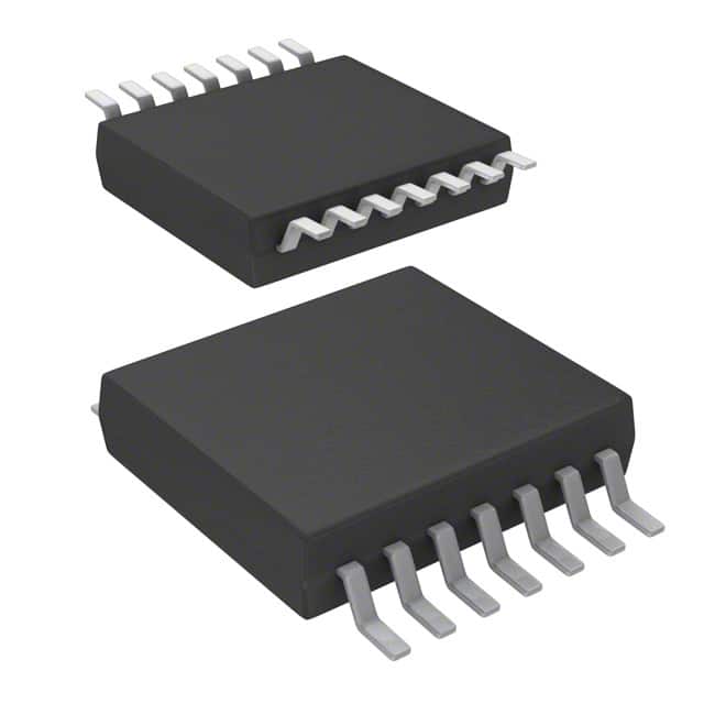
- Package: VSSOP (Very Small Outline Package)
- Essence: A multiplexer/demultiplexer IC that allows digital signals to be routed between multiple input/output channels
- Packaging/Quantity: Tape and Reel, 2500 units per reel
Specifications
- Supply Voltage Range: 2 V to 5.5 V
- Input/Output Voltage Range: 0 V to VCC
- On-State Resistance: 5 Ω (typical)
- Bandwidth: 400 MHz (typical)
- Number of Channels: 4
- Operating Temperature Range: -40°C to +85°C
Detailed Pin Configuration
- A0: Channel Select Input
- A1: Channel Select Input
- OE: Output Enable Input
- I/O0: Bidirectional Data I/O Channel 0
- I/O1: Bidirectional Data I/O Channel 1
- I/O2: Bidirectional Data I/O Channel 2
- I/O3: Bidirectional Data I/O Channel 3
- GND: Ground
- VCC: Power Supply
Functional Features
- Bidirectional switching: Allows routing of digital signals in both directions
- Low power consumption: Operates at a low supply voltage range, reducing power consumption
- High-speed operation: Supports high-frequency signals with a bandwidth of up to 400 MHz
- Channel selection: Controlled by the A0 and A1 inputs to select one of the four channels
- Output enable: The OE input enables or disables the outputs
Advantages and Disadvantages
Advantages: - High-speed operation allows for efficient signal routing - Low power consumption extends battery life in portable devices - Small package size saves board space - Bidirectional switching simplifies circuit design
Disadvantages: - Limited number of channels (4) - May not be suitable for applications requiring a higher number of channels
Working Principles
The SN74CBT3126DGVRG4 is based on CMOS technology and operates as a multiplexer/demultiplexer. It uses channel selection inputs (A0 and A1) to determine the desired input/output channel. The output enable input (OE) enables or disables the outputs. When enabled, the selected input channel is connected to the corresponding output channel bidirectionally.
Detailed Application Field Plans
- Data communication systems: The SN74CBT3126DGVRG4 can be used in data switches and routers to route digital signals between different channels.
- Test and measurement equipment: It can be utilized in test equipment to switch signals between various test points.
- Audio/video systems: The IC can be employed in audio/video switchers to select different audio/video sources.
- Industrial automation: It can be integrated into industrial control systems to route digital signals between different components.
Detailed and Complete Alternative Models
- SN74CBT3257CDBQR: Similar functionality with 8 channels instead of 4.
- SN74CBT16211ADGGR: Offers 16 channels with similar characteristics.
- SN74CBT3384ADBQR: Provides 8 channels with additional voltage level translation capabilities.
(Note: This list is not exhaustive and there are other alternative models available in the market.)
Word count: 399 words
Lista 10 Vanliga frågor och svar relaterade till tillämpningen av SN74CBT3126DGVRG4 i tekniska lösningar
Sure! Here are 10 common questions and answers related to the application of SN74CBT3126DGVRG4 in technical solutions:
Q: What is the SN74CBT3126DGVRG4? A: The SN74CBT3126DGVRG4 is a high-speed, low-power quad FET bus switch designed for use in various digital applications.
Q: What is the maximum voltage rating for the SN74CBT3126DGVRG4? A: The SN74CBT3126DGVRG4 has a maximum voltage rating of 3.6V.
Q: How many channels does the SN74CBT3126DGVRG4 have? A: The SN74CBT3126DGVRG4 has four independent bidirectional channels.
Q: What is the typical on-resistance of each channel in the SN74CBT3126DGVRG4? A: The typical on-resistance of each channel in the SN74CBT3126DGVRG4 is around 5 ohms.
Q: Can the SN74CBT3126DGVRG4 be used for level shifting between different voltage domains? A: Yes, the SN74CBT3126DGVRG4 can be used for level shifting between different voltage domains as long as the voltage levels are within its specified range.
Q: What is the maximum data rate supported by the SN74CBT3126DGVRG4? A: The SN74CBT3126DGVRG4 supports a maximum data rate of up to 400 Mbps.
Q: Does the SN74CBT3126DGVRG4 have built-in ESD protection? A: Yes, the SN74CBT3126DGVRG4 has built-in ESD protection to safeguard against electrostatic discharge.
Q: Can the SN74CBT3126DGVRG4 be used in both analog and digital applications? A: The SN74CBT3126DGVRG4 is primarily designed for digital applications, but it can also be used in certain analog applications within its specified parameters.
Q: What is the power supply voltage range for the SN74CBT3126DGVRG4? A: The power supply voltage range for the SN74CBT3126DGVRG4 is typically between 2V and 3.6V.
Q: Is the SN74CBT3126DGVRG4 available in different package options? A: Yes, the SN74CBT3126DGVRG4 is available in various package options, including the VSSOP-14 package.
Please note that these answers are general and may vary depending on the specific application and requirements. It's always recommended to refer to the datasheet and consult with the manufacturer for detailed information.