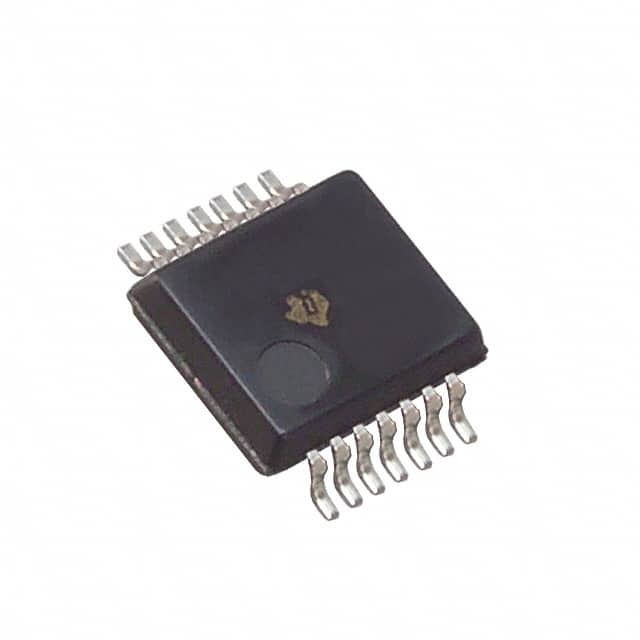
SN74F08DBR
Product Overview
- Category: Integrated Circuit (IC)
- Use: Logic Gate
- Characteristics: Quad 2-input AND gate
- Package: SSOP-14
- Essence: High-speed CMOS technology
- Packaging/Quantity: Tape and Reel, 2500 pieces per reel
Specifications
- Logic Family: F series
- Logic Type: AND gate
- Number of Gates: 4
- Number of Inputs: 2 per gate
- Input Voltage: 0V to 5.5V
- Output Voltage: 0V to 5.5V
- Propagation Delay: 3.5ns (typical)
- Operating Temperature Range: -40°C to 85°C
Detailed Pin Configuration
The SN74F08DBR has a SSOP-14 package with the following pin configuration:
- Input A1
- Input B1
- Output Y1
- Ground
- Input A2
- Input B2
- Output Y2
- VCC
- Input A3
- Input B3
- Output Y3
- Input A4
- Input B4
- Output Y4
Functional Features
- Quad 2-input AND gate: The SN74F08DBR consists of four independent AND gates, each with two inputs and one output.
- High-speed operation: Utilizing high-speed CMOS technology, this IC provides fast logic gate functionality.
- Wide voltage range: The input and output voltage levels can range from 0V to 5.5V, making it compatible with various systems.
- Low propagation delay: With a typical propagation delay of 3.5ns, this IC ensures efficient signal processing.
Advantages and Disadvantages
Advantages
- Compact package: The SSOP-14 package allows for space-saving integration into electronic circuits.
- Versatile use: The quad 2-input AND gate design enables flexible logic operations in a wide range of applications.
- High-speed performance: The use of high-speed CMOS technology ensures fast and reliable operation.
Disadvantages
- Limited number of gates: With only four gates, the SN74F08DBR may not be suitable for complex logic designs requiring a larger number of gates.
- Temperature limitations: The operating temperature range of -40°C to 85°C may restrict its use in extreme temperature environments.
Working Principles
The SN74F08DBR operates based on the principles of digital logic. Each of the four independent AND gates receives two input signals and produces an output signal based on the logical AND operation. The inputs and outputs are compatible with a wide voltage range, allowing seamless integration into various systems.
Detailed Application Field Plans
The SN74F08DBR can be used in a variety of applications, including:
- Digital electronics: It can be utilized in digital circuits for logical operations, such as data processing, arithmetic calculations, and control functions.
- Microcontrollers: This IC can be integrated into microcontroller-based systems to perform logical operations and interface with other components.
- Communication systems: It can be employed in communication systems for signal conditioning, error detection, and protocol implementation.
- Industrial automation: The SN74F08DBR can be used in industrial automation systems for controlling sensors, actuators, and logic-based decision-making.
Detailed and Complete Alternative Models
- SN74LS08N: Quad 2-input AND gate, DIP-14 package
- CD4081BE: Quad 2-input AND gate, DIP-14 package
- 74HC08D: Quad 2-input AND gate, SOIC-14 package
- CD74HCT08E: Quad 2-input AND gate, DIP-14 package
These alternative models offer similar functionality to the SN74F08DBR and can be considered as replacements based on specific requirements.
Word count: 439 words
Lista 10 Vanliga frågor och svar relaterade till tillämpningen av SN74F08DBR i tekniska lösningar
Sure! Here are 10 common questions and answers related to the application of SN74F08DBR in technical solutions:
Q: What is SN74F08DBR? A: SN74F08DBR is a quad 2-input AND gate integrated circuit (IC) from Texas Instruments.
Q: What is the purpose of SN74F08DBR? A: SN74F08DBR is used to perform logical AND operations on two input signals, producing an output signal based on their logical states.
Q: What is the voltage supply range for SN74F08DBR? A: The voltage supply range for SN74F08DBR is typically between 4.5V and 5.5V.
Q: What is the maximum operating frequency of SN74F08DBR? A: SN74F08DBR can operate at frequencies up to 100 MHz.
Q: How many inputs does SN74F08DBR have? A: SN74F08DBR has four independent 2-input AND gates, totaling eight input pins.
Q: Can SN74F08DBR be used with both TTL and CMOS logic families? A: Yes, SN74F08DBR is compatible with both TTL and CMOS logic families.
Q: What is the output drive capability of SN74F08DBR? A: SN74F08DBR has a typical output drive capability of 8 mA.
Q: Is SN74F08DBR suitable for high-speed applications? A: Yes, SN74F08DBR is designed for high-speed operation and is commonly used in applications requiring fast logic gates.
Q: Can SN74F08DBR be used in both digital and analog circuits? A: No, SN74F08DBR is specifically designed for digital logic applications and is not suitable for analog circuits.
Q: What are some common applications of SN74F08DBR? A: SN74F08DBR is commonly used in digital systems, such as microprocessors, memory interfaces, data communication, and control systems, where logical AND operations are required.
Please note that these answers are general and may vary depending on specific application requirements.


