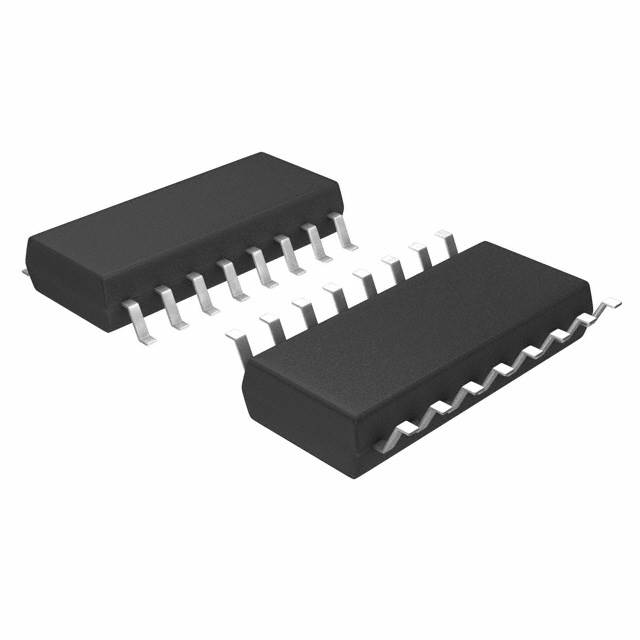
SN74HC365NSR
Product Overview
- Category: Integrated Circuit (IC)
- Use: Logic Level Converter
- Characteristics: High-Speed, Non-Inverting, Tri-State Outputs
- Package: SOIC (Small Outline Integrated Circuit)
- Essence: This IC is designed to convert logic level signals between different voltage levels.
- Packaging/Quantity: Tape and Reel, 2500 pieces per reel
Specifications
- Supply Voltage: 2V to 6V
- Input Voltage: 0V to VCC
- Output Voltage: 0V to VCC
- Operating Temperature Range: -40°C to +85°C
- Propagation Delay: 10 ns (typical)
- Output Current: ±8 mA
Detailed Pin Configuration
The SN74HC365NSR has a total of 16 pins. The pin configuration is as follows:
- A1: Input A1
- B1: Input B1
- Y1: Output Y1
- GND: Ground
- A2: Input A2
- B2: Input B2
- Y2: Output Y2
- OE: Output Enable
- VCC: Supply Voltage
- A3: Input A3
- B3: Input B3
- Y3: Output Y3
- A4: Input A4
- B4: Input B4
- Y4: Output Y4
- GND: Ground
Functional Features
- Non-inverting tri-state outputs allow bidirectional data flow.
- High-speed operation enables efficient signal conversion.
- Wide supply voltage range provides flexibility in various applications.
- Output enable pin allows for easy control of the output state.
Advantages and Disadvantages
Advantages: - High-speed operation ensures quick signal conversion. - Non-inverting outputs simplify data flow management. - Wide supply voltage range allows for versatile applications.
Disadvantages: - Limited output current may restrict usage in certain high-power applications. - Propagation delay of 10 ns may introduce slight timing issues in critical systems.
Working Principles
The SN74HC365NSR operates as a logic level converter by accepting input signals at different voltage levels and converting them to a desired output voltage level. The non-inverting tri-state outputs enable bidirectional data flow, making it suitable for various communication protocols. The output enable pin controls the state of the outputs, allowing for easy control of the signal flow.
Detailed Application Field Plans
The SN74HC365NSR can be used in a wide range of applications, including:
- Microcontroller interfacing with different voltage level peripherals.
- Communication systems requiring bidirectional data transfer.
- Level shifting in mixed-voltage systems.
- Signal conversion in industrial automation.
- Interface translation in automotive electronics.
Detailed and Complete Alternative Models
- SN74LVC1T45DBVR: Single-Bit Dual-Supply Bus Transceiver
- SN74LVCH245ADBR: Octal Bus Transceiver with 3-State Outputs
- SN74HCT125N: Quad Bus Buffer Gates with 3-State Outputs
- SN74LVC8T245PWR: 8-Bit Dual-Supply Bus Transceiver with Configurable Voltage Translation
These alternative models offer similar functionality and can be considered as alternatives to the SN74HC365NSR based on specific application requirements.
Word count: 418 words
Lista 10 Vanliga frågor och svar relaterade till tillämpningen av SN74HC365NSR i tekniska lösningar
Sure! Here are 10 common questions and answers related to the application of SN74HC365NSR:
Q: What is SN74HC365NSR? A: SN74HC365NSR is a high-speed hex buffer/driver with 3-state outputs, commonly used in digital logic applications.
Q: What is the operating voltage range for SN74HC365NSR? A: The operating voltage range for SN74HC365NSR is typically between 2V and 6V.
Q: How many 3-state outputs does SN74HC365NSR have? A: SN74HC365NSR has six 3-state outputs, which can be independently controlled.
Q: What is the maximum output current that SN74HC365NSR can drive? A: SN74HC365NSR can drive up to 8mA of current per output pin.
Q: Can SN74HC365NSR be used as a level shifter? A: Yes, SN74HC365NSR can be used as a level shifter to convert signals between different voltage levels.
Q: Is SN74HC365NSR compatible with TTL logic levels? A: Yes, SN74HC365NSR is compatible with both CMOS and TTL logic levels.
Q: Can SN74HC365NSR be used in bus-oriented systems? A: Yes, SN74HC365NSR is commonly used in bus-oriented systems where multiple devices share a common data bus.
Q: Does SN74HC365NSR have built-in protection against short circuits? A: No, SN74HC365NSR does not have built-in protection against short circuits. External measures should be taken to prevent damage.
Q: What is the typical propagation delay of SN74HC365NSR? A: The typical propagation delay of SN74HC365NSR is around 10ns.
Q: Can SN74HC365NSR be used in high-speed applications? A: Yes, SN74HC365NSR is designed for high-speed operation and can be used in various high-frequency applications.
Please note that these answers are general and may vary depending on specific application requirements.


