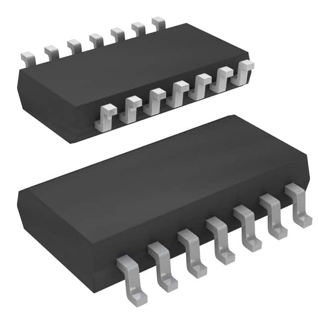
SN74LS00NSR
Product Overview
Category: Integrated Circuit (IC)
Use: The SN74LS00NSR is a quad 2-input NAND gate IC, which is widely used in digital logic circuits. It performs the logical operation of NAND (NOT AND) on two input signals.
Characteristics: - High-speed operation - Low power consumption - Wide operating voltage range - Compatible with TTL (Transistor-Transistor Logic) family
Package: The SN74LS00NSR is available in a small-outline package (SOIC), which consists of a plastic body with gull-wing leads for surface mount applications.
Essence: This IC is an essential component in various electronic devices and systems that require logical operations, such as computers, calculators, communication equipment, and control systems.
Packaging/Quantity: The SN74LS00NSR is typically sold in reels or tubes, containing a quantity of 250 or 3000 units per package.
Specifications
- Supply Voltage Range: 4.75V to 5.25V
- Input Voltage Range: 0V to Vcc
- Operating Temperature Range: -40°C to +85°C
- Propagation Delay Time: 9 ns (max)
- Output Current: ±8 mA
Detailed Pin Configuration
The SN74LS00NSR has a total of 14 pins, numbered as follows:
- A1 (Input A1)
- B1 (Input B1)
- Y1 (Output Y1)
- A2 (Input A2)
- B2 (Input B2)
- Y2 (Output Y2)
- GND (Ground)
- Y3 (Output Y3)
- B3 (Input B3)
- A3 (Input A3)
- Y4 (Output Y4)
- B4 (Input B4)
- A4 (Input A4)
- Vcc (Supply Voltage)
Functional Features
- Quad 2-input NAND gate: The SN74LS00NSR consists of four independent NAND gates, each with two inputs and one output.
- High-speed operation: It provides fast switching times, making it suitable for high-frequency applications.
- Low power consumption: The IC consumes minimal power, contributing to energy-efficient designs.
- TTL compatibility: It is designed to be compatible with other TTL logic families, allowing easy integration into existing systems.
Advantages and Disadvantages
Advantages: - Fast operation speed - Low power consumption - Wide operating voltage range - Compatibility with TTL family
Disadvantages: - Limited number of inputs per gate - Not suitable for high-voltage applications
Working Principles
The SN74LS00NSR operates based on the principle of NAND logic. It performs a logical NAND operation on the input signals, producing an inverted output. When both inputs are high (logic level 1), the output becomes low (logic level 0). In all other cases, the output remains high.
Detailed Application Field Plans
The SN74LS00NSR finds extensive use in various digital logic applications, including: - Arithmetic circuits - Data processing units - Memory systems - Control systems - Communication equipment - Industrial automation
Detailed and Complete Alternative Models
Some alternative models that can be used as substitutes for the SN74LS00NSR include: - 74HC00: High-speed CMOS quad 2-input NAND gate - CD4011: CMOS quad 2-input NAND gate - MC14011: CMOS quad 2-input NAND gate
These alternatives offer similar functionality and can be used interchangeably in most applications.
In conclusion, the SN74LS00NSR is a versatile quad 2-input NAND gate IC that provides high-speed operation, low power consumption, and compatibility with TTL logic. It finds widespread use in various digital logic circuits and offers advantages such as fast switching times and wide operating voltage range. However, it has limitations in terms of the number of inputs per gate and suitability for high-voltage applications.
Lista 10 Vanliga frågor och svar relaterade till tillämpningen av SN74LS00NSR i tekniska lösningar
Sure! Here are 10 common questions and answers related to the application of SN74LS00NSR:
Q: What is SN74LS00NSR? A: SN74LS00NSR is a quad 2-input NAND gate integrated circuit (IC) that is commonly used in digital logic circuits.
Q: What is the operating voltage range for SN74LS00NSR? A: The operating voltage range for SN74LS00NSR is typically between 4.75V and 5.25V.
Q: What is the maximum input voltage for SN74LS00NSR? A: The maximum input voltage for SN74LS00NSR is equal to the supply voltage, which is typically 5.25V.
Q: What is the output current capability of SN74LS00NSR? A: SN74LS00NSR has a typical output current capability of 8mA.
Q: Can SN74LS00NSR be used as a level shifter? A: Yes, SN74LS00NSR can be used as a level shifter to convert signals from one voltage level to another.
Q: How many gates are there in SN74LS00NSR? A: SN74LS00NSR contains four independent 2-input NAND gates.
Q: What is the propagation delay of SN74LS00NSR? A: The propagation delay of SN74LS00NSR is typically around 9 ns.
Q: Can SN74LS00NSR be used in high-speed applications? A: While SN74LS00NSR is not specifically designed for high-speed applications, it can still be used in moderate-speed digital circuits.
Q: Is SN74LS00NSR compatible with TTL logic levels? A: Yes, SN74LS00NSR is compatible with TTL (Transistor-Transistor Logic) logic levels.
Q: What are some common applications of SN74LS00NSR? A: SN74LS00NSR is commonly used in various digital logic circuits, such as counters, multiplexers, encoders, and more.
Please note that the answers provided here are general and may vary depending on specific datasheet specifications and application requirements.


