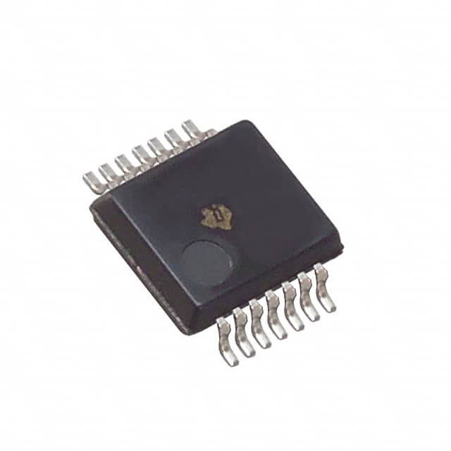
SN74LS06DBRG4
Product Overview
- Category: Integrated Circuit (IC)
- Use: Logic Gate
- Characteristics: Hex Inverter with Open-Collector Outputs
- Package: SOIC (Small Outline Integrated Circuit)
- Essence: The SN74LS06DBRG4 is a hex inverter IC that provides six independent inverters with open-collector outputs.
- Packaging/Quantity: Tape and Reel, 2500 units per reel
Specifications
- Supply Voltage Range: 4.75V to 5.25V
- High-Level Input Voltage: 2V to VCC
- Low-Level Input Voltage: 0V to 0.8V
- High-Level Output Voltage: 2.7V (min)
- Low-Level Output Voltage: 0.5V (max)
- Maximum Operating Frequency: 30 MHz
- Propagation Delay Time: 9 ns (typical)
Detailed Pin Configuration
The SN74LS06DBRG4 has a total of 14 pins, numbered as follows:
- A1 - Input for the first inverter
- Y1 - Output for the first inverter
- A2 - Input for the second inverter
- Y2 - Output for the second inverter
- A3 - Input for the third inverter
- Y3 - Output for the third inverter
- GND - Ground
- Y4 - Output for the fourth inverter
- A4 - Input for the fourth inverter
- Y5 - Output for the fifth inverter
- A5 - Input for the fifth inverter
- Y6 - Output for the sixth inverter
- A6 - Input for the sixth inverter
- VCC - Power supply voltage
Functional Features
- Hex Inverter: The SN74LS06DBRG4 consists of six independent inverters, each capable of converting a logic level input to its complement.
- Open-Collector Outputs: The outputs of the inverters are open-collector, allowing for wired-OR connections and easy interfacing with other devices.
- High-Speed Operation: With a maximum operating frequency of 30 MHz and a propagation delay time of 9 ns, the SN74LS06DBRG4 offers fast and efficient logic gate functionality.
Advantages and Disadvantages
Advantages: - Versatility: The hex inverter can be used in various digital logic applications. - Open-Collector Outputs: Allows for flexible circuit design and compatibility with different voltage levels. - High-Speed Operation: Suitable for applications requiring quick response times.
Disadvantages: - Power Consumption: The SN74LS06DBRG4 may consume more power compared to newer, low-power logic gate alternatives. - Limited Voltage Range: The supply voltage range is relatively narrow, which may restrict its use in certain applications.
Working Principles
The SN74LS06DBRG4 operates based on the principle of inverting the input logic level. Each inverter within the IC takes an input signal and produces the logical complement at its output. The open-collector outputs enable the connection of multiple outputs together, facilitating wired-OR configurations.
Detailed Application Field Plans
The SN74LS06DBRG4 finds applications in various fields, including:
- Digital Electronics: Used as a basic building block for logic circuits, such as flip-flops, counters, and registers.
- Communication Systems: Employed in signal conditioning, level shifting, and interfacing between different logic families.
- Industrial Control Systems: Utilized for control and monitoring functions in automation systems.
- Automotive Electronics: Integrated into automotive modules for signal processing and control purposes.
- Consumer Electronics: Found in devices like TVs, audio systems, and gaming consoles for signal manipulation and processing.
Detailed and Complete Alternative Models
- SN74LS04: Hex Inverter with TTL-level outputs.
- SN74HC06: Hex Inverter with CMOS-level outputs.
- SN74LVC06A: Hex Inverter with low-voltage CMOS-level outputs.
- SN74LVU04A: Hex Inverter with open-drain outputs.
These alternative models offer similar functionality to the SN74LS06DBRG4 but may differ in terms of voltage levels, power consumption, or package type.
Word count: 455 words
Lista 10 Vanliga frågor och svar relaterade till tillämpningen av SN74LS06DBRG4 i tekniska lösningar
Sure! Here are 10 common questions and answers related to the application of SN74LS06DBRG4 in technical solutions:
Q: What is SN74LS06DBRG4? A: SN74LS06DBRG4 is a hex inverter with open-drain outputs, which means it can invert input signals and provide an open-drain output.
Q: What is the voltage supply range for SN74LS06DBRG4? A: The voltage supply range for SN74LS06DBRG4 is typically between 4.75V and 5.25V.
Q: What is the maximum operating frequency of SN74LS06DBRG4? A: The maximum operating frequency of SN74LS06DBRG4 is typically around 30 MHz.
Q: Can SN74LS06DBRG4 be used as a level shifter? A: Yes, SN74LS06DBRG4 can be used as a level shifter by connecting its inputs and outputs to different voltage domains.
Q: How many inverters are there in SN74LS06DBRG4? A: SN74LS06DBRG4 has six independent inverters in a single package.
Q: What is the maximum current that SN74LS06DBRG4 can sink? A: SN74LS06DBRG4 can sink a maximum current of 8 mA per output.
Q: Can SN74LS06DBRG4 be used in high-speed applications? A: While SN74LS06DBRG4 is not specifically designed for high-speed applications, it can still be used in moderate-speed digital circuits.
Q: Is SN74LS06DBRG4 compatible with TTL logic levels? A: Yes, SN74LS06DBRG4 is compatible with TTL logic levels and can be used in TTL-compatible circuits.
Q: Can SN74LS06DBRG4 drive capacitive loads? A: SN74LS06DBRG4 can drive small capacitive loads, but for larger capacitive loads, it is recommended to use a buffer or driver.
Q: What is the temperature range for SN74LS06DBRG4? A: SN74LS06DBRG4 has an operating temperature range of -40°C to 85°C.
Please note that these answers are general and may vary depending on specific datasheet specifications and application requirements.


