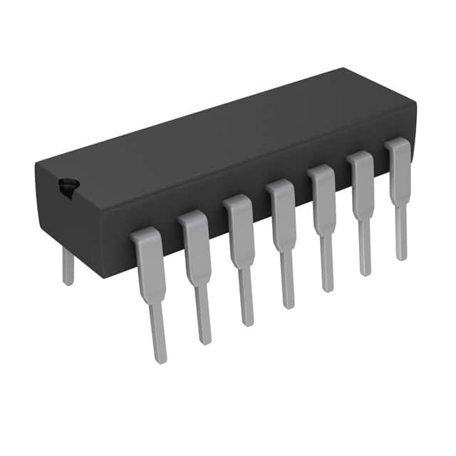
SN74LS38NG4
Product Overview
- Category: Integrated Circuit (IC)
- Use: Logic Gate
- Characteristics: Quad 2-input NAND Buffer
- Package: DIP-14 (Dual In-line Package with 14 pins)
- Essence: The SN74LS38NG4 is a logic gate IC that contains four 2-input NAND buffers. It is designed to provide high-speed, low-power logic functions for various digital applications.
- Packaging/Quantity: The SN74LS38NG4 is typically available in reels or tubes, with a quantity of 250 or 1,000 units per package.
Specifications
- Supply Voltage: 4.75V to 5.25V
- Input Voltage: 0V to VCC
- Output Voltage: 0V to VCC
- Operating Temperature Range: -40°C to +85°C
- Propagation Delay Time: 9ns (max)
- Power Dissipation: 22mW (typ)
Pin Configuration
The SN74LS38NG4 has a DIP-14 package with the following pin configuration:
__    __
   A1 | 1  14 | VCC
   B1 | 2  13 | Y1
   A2 | 3  12 | Y2
   B2 | 4  11 | Y3
   A3 | 5  10 | Y4
   B3 | 6   9 | GND
   Y0 | 7   8 | B4
       --------
Functional Features
- Quad 2-input NAND buffer: The SN74LS38NG4 consists of four independent 2-input NAND buffers, which can be used to perform logical operations on two input signals.
- High-speed operation: With a propagation delay time of only 9ns, the SN74LS38NG4 ensures fast response times in digital circuits.
- Low-power consumption: The IC is designed to operate with low power dissipation, making it suitable for battery-powered devices and energy-efficient applications.
Advantages and Disadvantages
Advantages
- Compact design: The DIP-14 package allows for easy integration into various circuit designs.
- Versatile functionality: The quad 2-input NAND buffer provides flexibility in implementing logical operations.
- High-speed performance: The low propagation delay time enables efficient data processing.
Disadvantages
- Limited number of inputs: The SN74LS38NG4 supports only two inputs per NAND gate, which may restrict complex logic operations requiring more inputs.
- Temperature limitations: The operating temperature range of -40°C to +85°C may not be suitable for extreme environments.
Working Principles
The SN74LS38NG4 operates based on the principles of NAND logic gates. Each of the four independent NAND buffers takes two input signals and produces an inverted output. The outputs are determined by the logical combination of the inputs according to the NAND truth table.
Detailed Application Field Plans
The SN74LS38NG4 can be used in various digital applications, including:
- Arithmetic circuits
- Data processing systems
- Control systems
- Communication devices
- Industrial automation
Detailed and Complete Alternative Models
Some alternative models that provide similar functionality to the SN74LS38NG4 include:
- SN74LS00N: Quad 2-input NAND Gate
- SN74LS02N: Quad 2-input NOR Gate
- SN74LS04N: Hex Inverter
- SN74LS08N: Quad 2-input AND Gate
- SN74LS32N: Quad 2-input OR Gate
These alternative models offer different logic gate functions and can be chosen based on specific application requirements.
In conclusion, the SN74LS38NG4 is a quad 2-input NAND buffer IC that provides high-speed, low-power logic functions. Its compact design, versatile functionality, and fast performance make it suitable for various digital applications. However, its limited number of inputs and temperature limitations should be considered when selecting this IC for specific projects.
Lista 10 Vanliga frågor och svar relaterade till tillämpningen av SN74LS38NG4 i tekniska lösningar
Sure! Here are 10 common questions and answers related to the application of SN74LS38NG4 in technical solutions:
Q: What is SN74LS38NG4? A: SN74LS38NG4 is a quad 2-input NAND buffer/driver IC (integrated circuit) commonly used in digital logic applications.
Q: What is the purpose of SN74LS38NG4? A: SN74LS38NG4 is used to provide buffering and driving capabilities for digital signals, allowing them to be properly transmitted and received between different components or subsystems.
Q: What voltage levels does SN74LS38NG4 support? A: SN74LS38NG4 operates with a supply voltage range of 4.75V to 5.25V, making it compatible with standard TTL (Transistor-Transistor Logic) voltage levels.
Q: How many inputs does SN74LS38NG4 have? A: SN74LS38NG4 has four independent 2-input NAND gates, providing a total of eight input pins.
Q: Can SN74LS38NG4 be used for level shifting? A: No, SN74LS38NG4 is not designed for level shifting as it operates at TTL voltage levels. For level shifting, you would need to use ICs specifically designed for that purpose, such as level shifters or voltage translators.
Q: What is the maximum current that SN74LS38NG4 can source or sink? A: SN74LS38NG4 can typically source or sink up to 8mA of current per output pin.
Q: Is SN74LS38NG4 suitable for high-speed applications? A: While SN74LS38NG4 is capable of operating at moderate speeds, it is not optimized for high-speed applications. For such cases, you may consider using ICs specifically designed for high-speed logic, like the LS-TTL (Low-Power Schottky Transistor-Transistor Logic) family.
Q: Can SN74LS38NG4 be used in both digital and analog circuits? A: No, SN74LS38NG4 is designed specifically for digital logic applications and should not be used in analog circuits.
Q: What is the temperature range within which SN74LS38NG4 can operate? A: SN74LS38NG4 has an operating temperature range of 0°C to 70°C.
Q: Are there any specific precautions to take when using SN74LS38NG4? A: It is important to ensure proper decoupling and bypassing of power supply pins, avoid exceeding the maximum voltage and current ratings, and follow the recommended layout guidelines provided in the datasheet to minimize noise and signal integrity issues.
Please note that these answers are general and may vary depending on the specific application and requirements. Always refer to the manufacturer's datasheet and guidelines for accurate information.


