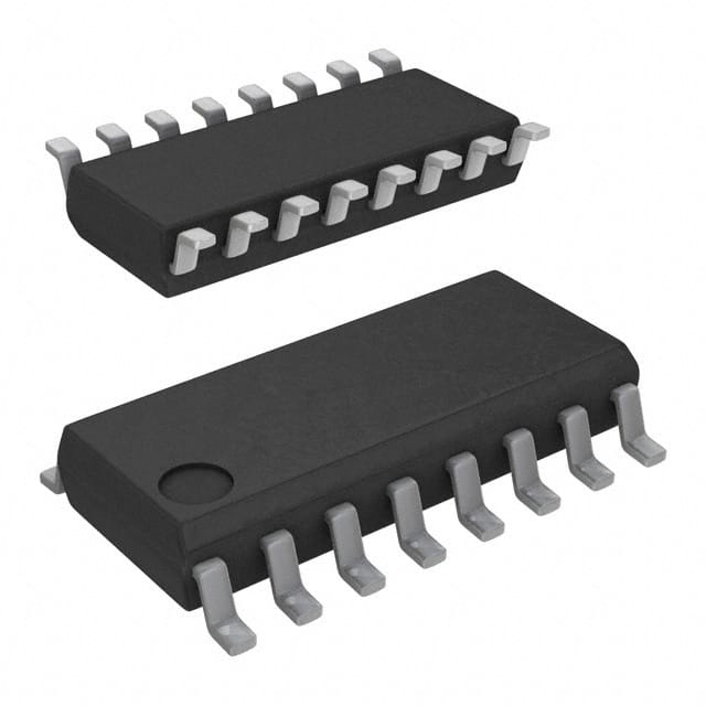
SN74LS76ADR
Product Overview
- Category: Integrated Circuit (IC)
- Use: Flip-Flop
- Characteristics: Dual J-K Flip-Flop with Clear and Preset
- Package: SOIC-16
- Essence: The SN74LS76ADR is a dual J-K flip-flop IC that provides the functionality of two individual J-K flip-flops in a single package.
- Packaging/Quantity: Available in reels of 2500 pieces or tubes of 50 pieces.
Specifications
- Supply Voltage Range: 4.75V to 5.25V
- High-Level Input Voltage: 2V (min), 7V (max)
- Low-Level Input Voltage: -0.5V (min), 0.8V (max)
- High-Level Output Voltage: 2.7V (min), VCC (max)
- Low-Level Output Voltage: 0.5V (max)
- Maximum Operating Frequency: 33 MHz
- Propagation Delay Time: 15 ns (typical)
Detailed Pin Configuration
The SN74LS76ADR has a total of 16 pins, which are assigned specific functions as follows:
- CLR (Clear) - Active low clear input pin for resetting the flip-flop.
- CP (Clock Pulse) - Clock input pin for triggering the flip-flop.
- J (J Input) - J input pin for setting the flip-flop output based on the clock pulse.
- K (K Input) - K input pin for resetting the flip-flop output based on the clock pulse.
- Q1 (Output 1) - Output pin for the first flip-flop.
- Q1' (Complementary Output 1) - Complementary output pin for the first flip-flop.
- GND (Ground) - Ground reference pin.
- Q2 (Output 2) - Output pin for the second flip-flop.
- Q2' (Complementary Output 2) - Complementary output pin for the second flip-flop.
- PRE (Preset) - Active low preset input pin for setting the flip-flop output.
- CPD (Clock Pulse Disable) - Clock pulse disable input pin for disabling the clock pulse.
- NC (No Connection) - No connection pin.
- NC (No Connection) - No connection pin.
- VCC (Positive Power Supply) - Positive power supply pin.
- NC (No Connection) - No connection pin.
- NC (No Connection) - No connection pin.
Functional Features
- Dual J-K Flip-Flop: The SN74LS76ADR integrates two independent J-K flip-flops in a single package, allowing for compact circuit designs.
- Clear and Preset Inputs: The IC provides clear and preset inputs to easily reset or set the flip-flop outputs.
- Clock Pulse Triggered: The flip-flop outputs are updated based on the rising edge of the clock pulse input.
- Complementary Outputs: Each flip-flop has a complementary output, providing both true and inverted outputs.
Advantages and Disadvantages
Advantages: - Compact Design: Integration of two flip-flops in a single package saves board space. - Clear and Preset Functionality: Easy control over the flip-flop outputs. - Complementary Outputs: Provides flexibility in circuit design.
Disadvantages: - Limited Operating Frequency: Maximum operating frequency of 33 MHz may not be suitable for high-speed applications. - Single Package: Failure of one flip-flop affects the functionality of both.
Working Principles
The SN74LS76ADR operates as a synchronous dual J-K flip-flop. The flip-flop outputs are updated based on the rising edge of the clock pulse input. The J and K inputs determine the output state based on the current state and the clock pulse. The clear and preset inputs allow for easy resetting or setting of the flip-flop outputs.
Detailed Application Field Plans
The SN74LS76ADR can be used in various applications, including: - Sequential Logic Circuits - Counters and Registers - Data Storage and Transfer Systems - Control Systems
Detailed and Complete Alternative Models
Some alternative models to the SN74LS76ADR include: - 74HC76: Dual J-K Flip-Flop with Clear and Preset (CMOS technology) - CD4027: Dual J-K Master-Slave Flip-Flop with Set and Reset (CMOS technology) - MC14027B: Dual J-K Master-Slave Flip-Flop with Set and Reset (TTL technology)
These alternative models offer similar functionality but may have different specifications and pin configurations.
Word count: 523 words
Lista 10 Vanliga frågor och svar relaterade till tillämpningen av SN74LS76ADR i tekniska lösningar
Sure! Here are 10 common questions and answers related to the application of SN74LS76ADR:
Q: What is SN74LS76ADR? A: SN74LS76ADR is a dual J-K flip-flop integrated circuit (IC) that can be used in various digital applications.
Q: What is the operating voltage range for SN74LS76ADR? A: The operating voltage range for SN74LS76ADR is typically between 4.75V and 5.25V.
Q: What is the maximum clock frequency supported by SN74LS76ADR? A: SN74LS76ADR can support clock frequencies up to 30 MHz.
Q: How many flip-flops are there in SN74LS76ADR? A: SN74LS76ADR contains two independent J-K flip-flops.
Q: What is the purpose of the J and K inputs in SN74LS76ADR? A: The J and K inputs are used to control the state of the flip-flops and determine the output based on the clock signal.
Q: Can SN74LS76ADR be used in synchronous or asynchronous mode? A: SN74LS76ADR can be used in both synchronous and asynchronous modes, depending on the application requirements.
Q: What is the typical propagation delay of SN74LS76ADR? A: The typical propagation delay of SN74LS76ADR is around 15 ns.
Q: Can SN74LS76ADR be cascaded to create larger counters or shift registers? A: Yes, SN74LS76ADR can be cascaded with other flip-flops to create larger counters or shift registers.
Q: What is the power supply current consumption of SN74LS76ADR? A: The power supply current consumption of SN74LS76ADR is typically around 8 mA.
Q: What are some common applications of SN74LS76ADR? A: SN74LS76ADR can be used in applications such as frequency dividers, counters, shift registers, and general-purpose digital logic circuits.
Please note that the answers provided here are general and may vary depending on specific datasheet specifications or application requirements.


