

SN74LV10ADGVRE4
Product Overview
- Category: Integrated Circuit
- Use: Logic Gate
- Characteristics: Triple 3-Input Positive-NAND Gate
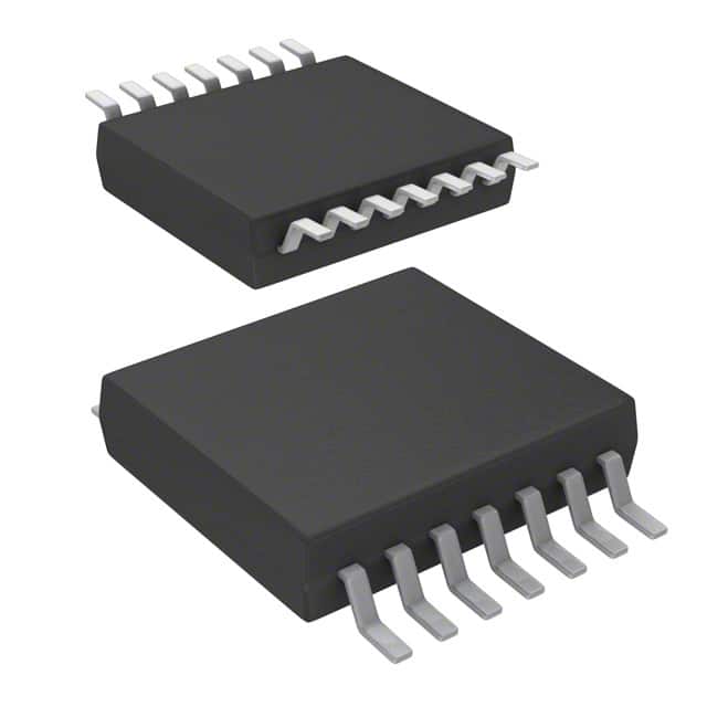
- Package: VSON (Very Small Outline No Lead)
- Essence: High-performance digital logic gate
- Packaging/Quantity: Tape and Reel, 2500 pieces per reel
Specifications
- Supply Voltage Range: 1.65V to 5.5V
- Input Voltage Range: -0.5V to VCC + 0.5V
- Output Voltage Range: 0V to VCC
- Operating Temperature Range: -40°C to 85°C
- Propagation Delay Time: 6.2ns (typical)
- Maximum Operating Frequency: 100MHz
Detailed Pin Configuration
The SN74LV10ADGVRE4 has a total of 14 pins arranged as follows:
- Pin 1: Input A
- Pin 2: Input B
- Pin 3: Input C
- Pin 4: Ground (GND)
- Pin 5: Output Y
- Pin 6: Output Y
- Pin 7: Output Y
- Pin 8: VCC (Positive Power Supply)
- Pin 9: Output Enable (OE)
- Pin 10: Input A
- Pin 11: Input B
- Pin 12: Input C
- Pin 13: Ground (GND)
- Pin 14: Output Y
Functional Features
- Triple 3-input positive-NAND gate with open-drain outputs
- Low power consumption
- Wide operating voltage range
- High-speed operation
- Schmitt-trigger inputs for noise immunity
- Compatible with TTL and CMOS logic levels
Advantages and Disadvantages
Advantages: - Low power consumption makes it suitable for battery-powered devices - Wide operating voltage range allows for compatibility with various systems - High-speed operation enables efficient data processing - Schmitt-trigger inputs provide noise immunity, ensuring reliable operation - Compatibility with TTL and CMOS logic levels simplifies integration into existing designs
Disadvantages: - Limited number of inputs (3-input gate) - Open-drain outputs may require additional circuitry for certain applications
Working Principles
The SN74LV10ADGVRE4 is a triple 3-input positive-NAND gate. It performs the logical NAND operation on three input signals (A, B, and C) and provides the corresponding output signal (Y). The open-drain outputs allow for flexible connection to other components in the system.
The gate operates based on the principles of digital logic, where logical operations are performed using binary signals. In the case of the NAND gate, the output is low (logic 0) only when all three inputs are high (logic 1). Otherwise, the output is high (logic 1).
Detailed Application Field Plans
The SN74LV10ADGVRE4 can be used in various applications that require logical operations. Some potential application fields include:
- Digital Systems: The gate can be used in microcontrollers, digital signal processors, and other digital systems to perform logical operations.
- Communication Systems: It can be utilized in communication systems for error detection, data encoding/decoding, and protocol implementation.
- Industrial Automation: The gate finds applications in industrial automation systems for control and monitoring purposes.
- Automotive Electronics: It can be employed in automotive electronics for functions like sensor interfacing, signal conditioning, and control unit logic.
Detailed and Complete Alternative Models
- SN74LV10APWR: Similar triple 3-input positive-NAND gate with different package (TSSOP)
- SN74LV10ADR: Triple 3-input positive-NAND gate with different package (SOIC)
- SN74LV10ANSR: Triple 3-input positive-NAND gate with different package (SOT-23)
These alternative models offer similar functionality and can be used as substitutes for the SN74LV10ADGVRE4 in various applications.
Word count: 511 words
Lista 10 Vanliga frågor och svar relaterade till tillämpningen av SN74LV10ADGVRE4 i tekniska lösningar
Sure! Here are 10 common questions and answers related to the application of SN74LV10ADGVRE4 in technical solutions:
Q: What is SN74LV10ADGVRE4? A: SN74LV10ADGVRE4 is a triple 3-input positive-NAND gate integrated circuit (IC) that can be used in various digital logic applications.
Q: What is the operating voltage range for SN74LV10ADGVRE4? A: The operating voltage range for SN74LV10ADGVRE4 is typically between 1.65V and 5.5V.
Q: Can SN74LV10ADGVRE4 be used in battery-powered devices? A: Yes, SN74LV10ADGVRE4 can be used in battery-powered devices as it operates at low voltages and has low power consumption.
Q: What is the maximum output current of SN74LV10ADGVRE4? A: The maximum output current of SN74LV10ADGVRE4 is typically around 8mA.
Q: Can SN74LV10ADGVRE4 be used in high-speed applications? A: No, SN74LV10ADGVRE4 is not designed for high-speed applications. It is more suitable for low to moderate speed digital logic circuits.
Q: Does SN74LV10ADGVRE4 have built-in protection against electrostatic discharge (ESD)? A: Yes, SN74LV10ADGVRE4 has built-in ESD protection to prevent damage from static electricity.
Q: How many inputs does SN74LV10ADGVRE4 have? A: SN74LV10ADGVRE4 has three inputs, allowing it to perform logical operations on three different signals.
Q: Can SN74LV10ADGVRE4 be used in both CMOS and TTL logic systems? A: Yes, SN74LV10ADGVRE4 is compatible with both CMOS and TTL logic levels, making it versatile for various applications.
Q: What is the typical propagation delay of SN74LV10ADGVRE4? A: The typical propagation delay of SN74LV10ADGVRE4 is around 5 nanoseconds (ns).
Q: Is SN74LV10ADGVRE4 available in surface mount packages? A: Yes, SN74LV10ADGVRE4 is available in a surface mount package (VRE4) for easy integration onto PCBs.
Please note that these answers are general and may vary depending on specific datasheet specifications and application requirements.