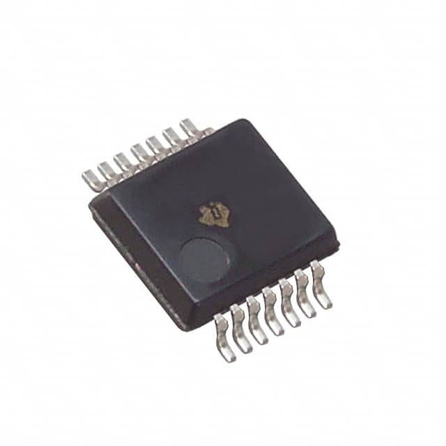
SN74LV11ADBR
Product Overview
Category
SN74LV11ADBR belongs to the category of integrated circuits (ICs).
Use
This IC is commonly used for logic gate applications.
Characteristics
- Low-voltage operation
- High-speed performance
- Wide operating temperature range
- Low power consumption
Package
SN74LV11ADBR is available in a small-outline package (SOIC) with 14 pins.
Essence
The essence of SN74LV11ADBR lies in its ability to perform logical operations efficiently and reliably.
Packaging/Quantity
SN74LV11ADBR is typically packaged in reels or tubes, with each reel/tube containing a specific quantity of ICs. The exact quantity may vary depending on the manufacturer's specifications.
Specifications
- Supply Voltage: 2V to 5.5V
- Logic Family: LV
- Number of Gates: 3
- Input Type: Schmitt Trigger
- Output Type: CMOS
- Operating Temperature Range: -40°C to +85°C
Detailed Pin Configuration
- A Input 1
- B Input 1
- Y Output 1
- A Input 2
- B Input 2
- Y Output 2
- GND (Ground)
- C Input 1
- D Input 1
- Y Output 3
- C Input 2
- D Input 2
- Y Output 4
- VCC (Power Supply)
Functional Features
- Triple 3-input positive-AND gates
- Schmitt-trigger inputs for improved noise immunity
- Compatible with various voltage levels
- Fast propagation delay for high-speed applications
Advantages and Disadvantages
Advantages
- Low-voltage operation allows for compatibility with modern electronic systems
- High-speed performance enables efficient data processing
- Wide operating temperature range ensures reliability in various environments
- Low power consumption contributes to energy efficiency
Disadvantages
- Limited number of gates (3) may restrict complex logic operations
- Schmitt-trigger inputs may introduce additional complexity in circuit design
Working Principles
SN74LV11ADBR operates based on the principles of digital logic. It utilizes three 3-input positive-AND gates to perform logical operations on input signals. The Schmitt-trigger inputs provide improved noise immunity, ensuring reliable operation even in the presence of electrical noise.
Detailed Application Field Plans
SN74LV11ADBR finds applications in various fields, including but not limited to: 1. Digital electronics 2. Communication systems 3. Industrial automation 4. Automotive electronics 5. Consumer electronics
In digital electronics, this IC can be used for signal conditioning, data processing, and control logic implementation. In communication systems, it can assist in signal modulation, demodulation, and error detection. In industrial automation, SN74LV11ADBR can be employed for process control, sensor interfacing, and logic-based decision making. In automotive electronics, it can contribute to vehicle control systems, safety features, and entertainment systems. Lastly, in consumer electronics, this IC can be utilized in devices such as smartphones, tablets, and gaming consoles for various logic-related functions.
Detailed and Complete Alternative Models
Some alternative models that offer similar functionality to SN74LV11ADBR include: 1. SN74HC11N 2. CD4073B 3. MC14011B 4. 74LS11
These alternatives are widely available and can be considered as replacements based on specific requirements and compatibility considerations.
Word count: 520 words
Lista 10 Vanliga frågor och svar relaterade till tillämpningen av SN74LV11ADBR i tekniska lösningar
Sure! Here are 10 common questions and answers related to the application of SN74LV11ADBR in technical solutions:
Q: What is SN74LV11ADBR? A: SN74LV11ADBR is a triple 3-input AND gate integrated circuit (IC) that can be used in various digital logic applications.
Q: What is the operating voltage range for SN74LV11ADBR? A: The operating voltage range for SN74LV11ADBR is typically between 1.65V and 5.5V.
Q: What is the maximum output current of SN74LV11ADBR? A: The maximum output current of SN74LV11ADBR is around 8mA.
Q: Can SN74LV11ADBR be used in high-speed applications? A: Yes, SN74LV11ADBR is designed for high-speed operation and can be used in applications with fast switching requirements.
Q: How many inputs does SN74LV11ADBR have? A: SN74LV11ADBR has three inputs, allowing it to perform logical AND operations on three different signals.
Q: What is the typical propagation delay of SN74LV11ADBR? A: The typical propagation delay of SN74LV11ADBR is around 5 nanoseconds.
Q: Can SN74LV11ADBR be used in both CMOS and TTL logic systems? A: Yes, SN74LV11ADBR is compatible with both CMOS and TTL logic levels, making it versatile for various system designs.
Q: What is the power supply voltage required for SN74LV11ADBR? A: SN74LV11ADBR requires a power supply voltage between 2V and 5.5V.
Q: Can SN74LV11ADBR be used in battery-powered applications? A: Yes, SN74LV11ADBR's low power consumption makes it suitable for battery-powered applications where energy efficiency is crucial.
Q: What package options are available for SN74LV11ADBR? A: SN74LV11ADBR is available in various package options, including SOIC (Small Outline Integrated Circuit) and TSSOP (Thin Shrink Small Outline Package).
Please note that the answers provided here are general and may vary depending on specific datasheet specifications and application requirements.


