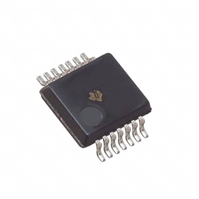
SN74LVC00ADBRE4
Product Overview
- Category: Integrated Circuit
- Use: Logic Gate
- Characteristics: Quad 2-Input NAND Gate
- Package: SOIC (Small Outline Integrated Circuit)
- Essence: High-speed CMOS technology
- Packaging/Quantity: Tape and Reel, 2500 pieces per reel
Specifications
- Supply Voltage Range: 1.65V to 5.5V
- Input Voltage Range: -0.5V to VCC + 0.5V
- Output Voltage Range: 0V to VCC
- Maximum Operating Frequency: 200MHz
- Propagation Delay: 3.8ns (typical)
- Low Power Consumption: ICC = 2μA (maximum)
Detailed Pin Configuration
The SN74LVC00ADBRE4 has a total of 14 pins. The pin configuration is as follows:
- A Input 1
- B Input 1
- Y Output 1
- GND (Ground)
- A Input 2
- B Input 2
- Y Output 2
- VCC (Supply Voltage)
- Y Output 3
- B Input 3
- A Input 3
- Y Output 4
- B Input 4
- A Input 4
Functional Features
- Quad 2-Input NAND Gate: The SN74LVC00ADBRE4 consists of four independent 2-input NAND gates in a single package.
- High-Speed Operation: Utilizing advanced CMOS technology, this IC offers high-speed performance with low power consumption.
- Wide Voltage Range: The supply voltage range of 1.65V to 5.5V allows for compatibility with various systems.
- Schmitt-Trigger Inputs: The inputs are equipped with Schmitt-trigger circuitry, ensuring reliable operation even in noisy environments.
- ESD Protection: The IC provides electrostatic discharge (ESD) protection, safeguarding against potential damage during handling and assembly.
Advantages and Disadvantages
Advantages: - High-speed operation enables efficient processing of logic signals. - Wide voltage range allows for compatibility with different power supply systems. - Schmitt-trigger inputs ensure reliable operation in noisy environments. - ESD protection enhances the durability and reliability of the IC.
Disadvantages: - Limited to quad 2-input NAND gate functionality, may not be suitable for applications requiring other logic functions. - May not be cost-effective for low-complexity projects that do not require multiple gates.
Working Principles
The SN74LVC00ADBRE4 operates based on the principles of CMOS technology. It utilizes a combination of NMOS and PMOS transistors to implement the NAND gate functionality. When both input signals are low, the output is high. If any of the input signals go high, the output becomes low. This behavior follows the logical operation of a NAND gate.
Detailed Application Field Plans
The SN74LVC00ADBRE4 finds application in various digital systems where NAND gate functionality is required. Some common application fields include:
- Digital Logic Design: The IC can be used in the design of complex digital circuits, such as arithmetic units, memory systems, and microprocessors.
- Communication Systems: It can be employed in communication systems for signal processing, error detection, and data encoding/decoding.
- Industrial Automation: The IC can be utilized in control systems, PLCs (Programmable Logic Controllers), and robotics for logical decision-making and control.
- Automotive Electronics: It finds application in automotive systems for signal conditioning, sensor interfacing, and control unit logic.
Detailed and Complete Alternative Models
- SN74LVC00APWR: This variant comes in a TSSOP (Thin Shrink Small Outline Package) package and offers similar functionality to the SN74LVC00ADBRE4.
- MC74VHC00DT: This alternative model is part of the VHC (Very High-Speed CMOS) logic family and provides quad 2-input NAND gates in an SOIC package.
- CD4011BE: This IC from the CD4000 series is a popular alternative, offering quad 2-input NAND gates in a DIP (Dual Inline Package) format.
These alternative models provide similar functionality to the SN74LVC00ADBRE4 and can be considered as replacements based on specific project requirements.
Word count: 550 words
Lista 10 Vanliga frågor och svar relaterade till tillämpningen av SN74LVC00ADBRE4 i tekniska lösningar
Sure! Here are 10 common questions and answers related to the application of SN74LVC00ADBRE4:
Q: What is SN74LVC00ADBRE4? A: SN74LVC00ADBRE4 is a quad 2-input NAND gate IC (integrated circuit) that is commonly used in digital logic applications.
Q: What is the operating voltage range for SN74LVC00ADBRE4? A: The operating voltage range for SN74LVC00ADBRE4 is typically between 1.65V and 5.5V.
Q: What is the maximum output current of SN74LVC00ADBRE4? A: The maximum output current of SN74LVC00ADBRE4 is 32mA per output.
Q: Can SN74LVC00ADBRE4 be used in both CMOS and TTL logic systems? A: Yes, SN74LVC00ADBRE4 is compatible with both CMOS and TTL logic systems.
Q: What is the propagation delay of SN74LVC00ADBRE4? A: The propagation delay of SN74LVC00ADBRE4 is typically around 4.3ns.
Q: Can SN74LVC00ADBRE4 be used in high-speed applications? A: Yes, SN74LVC00ADBRE4 is designed for high-speed operation and can be used in various high-speed applications.
Q: Does SN74LVC00ADBRE4 have built-in protection against electrostatic discharge (ESD)? A: Yes, SN74LVC00ADBRE4 has built-in ESD protection, which helps safeguard the IC from damage during handling and operation.
Q: Can SN74LVC00ADBRE4 drive capacitive loads? A: Yes, SN74LVC00ADBRE4 can drive capacitive loads up to 50pF.
Q: Is SN74LVC00ADBRE4 RoHS compliant? A: Yes, SN74LVC00ADBRE4 is RoHS (Restriction of Hazardous Substances) compliant, meaning it meets the environmental standards set by the European Union.
Q: What package options are available for SN74LVC00ADBRE4? A: SN74LVC00ADBRE4 is available in various package options, including SOIC (Small Outline Integrated Circuit) and TSSOP (Thin Shrink Small Outline Package).
Please note that these answers are general and may vary depending on specific datasheet specifications and manufacturer guidelines.


