

SN74LVC07ARGYRG4
Product Overview
- Category: Integrated Circuit (IC)
- Use: Buffer/Driver
- Characteristics: Low-Voltage CMOS Hex Buffer/Driver with 3-State Outputs
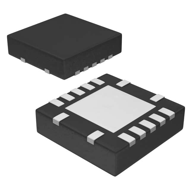
- Package: VQFN-16
- Essence: This IC is designed to provide buffering and driving capabilities for digital signals in low-voltage applications.
- Packaging/Quantity: Tape and Reel, 2500 units per reel
Specifications
- Supply Voltage Range: 1.65V to 5.5V
- High-Level Input Voltage: 2V to VCC + 0.5V
- Low-Level Input Voltage: -0.5V to 0.8V
- High-Level Output Voltage: VCC - 0.5V
- Low-Level Output Voltage: 0.5V
- Maximum Operating Frequency: 100MHz
- Propagation Delay: 3.7ns (typical)
Detailed Pin Configuration
The SN74LVC07ARGYRG4 has a VQFN-16 package with the following pin configuration:
__    __
   A1 | 1    16 | VCC
   A2 | 2    15 | Y1
   B1 | 3    14 | A3
   B2 | 4    13 | Y2
   C1 | 5    12 | A4
   C2 | 6    11 | Y3
  GND | 7    10 | A5
   Y4 | 8     9 | Y5
       ‾‾    ‾‾
Functional Features
- Hex buffer/driver with 3-state outputs
- Inputs are compatible with TTL and CMOS logic levels
- Provides buffering and driving capabilities for digital signals
- 3-state outputs allow multiple devices to share a common bus
Advantages and Disadvantages
Advantages: - Low-voltage operation makes it suitable for battery-powered applications - Wide supply voltage range allows compatibility with various systems - High-speed operation enables efficient signal processing - 3-state outputs facilitate bus sharing in multi-device systems
Disadvantages: - Limited number of buffer/driver channels (6 in total) - Not suitable for high-power applications due to low output current capability
Working Principles
The SN74LVC07ARGYRG4 operates based on complementary metal-oxide-semiconductor (CMOS) technology. It consists of six independent buffer/driver channels, each capable of providing both buffering and driving functions for digital signals. The inputs are compatible with both transistor-transistor logic (TTL) and CMOS logic levels, allowing seamless integration into various systems.
The IC operates within a wide supply voltage range of 1.65V to 5.5V, making it suitable for low-voltage applications, including battery-powered devices. It offers high-speed operation with a maximum operating frequency of 100MHz and a propagation delay of 3.7ns (typical).
The 3-state outputs of the SN74LVC07ARGYRG4 enable multiple devices to share a common bus. This feature is particularly useful in multi-device systems where several components need to communicate with each other without interfering with the bus when not actively transmitting data.
Detailed Application Field Plans
The SN74LVC07ARGYRG4 finds applications in various fields, including:
- Consumer Electronics: Used in smartphones, tablets, and portable media players for signal buffering and driving.
- Automotive: Employed in automotive electronics for signal conditioning and level shifting.
- Industrial Automation: Integrated into control systems and PLCs for signal amplification and isolation.
- Communication Systems: Utilized in networking equipment, routers, and switches for signal buffering and line driving.
- Medical Devices: Incorporated into medical instruments and diagnostic equipment for signal processing and amplification.
Detailed and Complete Alternative Models
- SN74LVC07APW: TSSOP-14 package, similar specifications and features.
- SN74LVC07ADGVR: TVSOP-14 package, similar specifications and features.
- SN74LVC07ADR: SOIC-14 package, similar specifications and features.
- SN74LVC07ARGYR: VQFN-16 package, similar specifications and features.
These alternative models offer similar functionality and can be used as replacements for the SN74LVC07ARGYRG4 depending on the specific requirements of the application.
Word count: 529 words
Lista 10 Vanliga frågor och svar relaterade till tillämpningen av SN74LVC07ARGYRG4 i tekniska lösningar
Sure! Here are 10 common questions and answers related to the application of SN74LVC07ARGYRG4:
Q: What is SN74LVC07ARGYRG4? A: SN74LVC07ARGYRG4 is a hex buffer/driver with open-drain outputs, commonly used in digital logic applications.
Q: What is the voltage range supported by SN74LVC07ARGYRG4? A: SN74LVC07ARGYRG4 supports a wide voltage range from 1.65V to 5.5V.
Q: What is the maximum output current of SN74LVC07ARGYRG4? A: The maximum output current per channel of SN74LVC07ARGYRG4 is typically 32mA.
Q: Can SN74LVC07ARGYRG4 be used for level shifting between different voltage domains? A: Yes, SN74LVC07ARGYRG4 can be used for level shifting as it supports multiple voltage levels.
Q: How many channels does SN74LVC07ARGYRG4 have? A: SN74LVC07ARGYRG4 has six independent buffer/driver channels.
Q: Is SN74LVC07ARGYRG4 suitable for bidirectional communication? A: No, SN74LVC07ARGYRG4 is not bidirectional. It only supports unidirectional communication.
Q: What is the typical propagation delay of SN74LVC07ARGYRG4? A: The typical propagation delay of SN74LVC07ARGYRG4 is around 4.3ns.
Q: Can SN74LVC07ARGYRG4 drive capacitive loads? A: Yes, SN74LVC07ARGYRG4 can drive capacitive loads up to 50pF.
Q: Does SN74LVC07ARGYRG4 have built-in protection features? A: Yes, SN74LVC07ARGYRG4 has built-in ESD protection on all inputs and outputs.
Q: What is the package type of SN74LVC07ARGYRG4? A: SN74LVC07ARGYRG4 is available in a small-outline integrated circuit (SOIC) package with 14 pins.
Please note that these answers are general and may vary depending on the specific datasheet and manufacturer's specifications for SN74LVC07ARGYRG4.