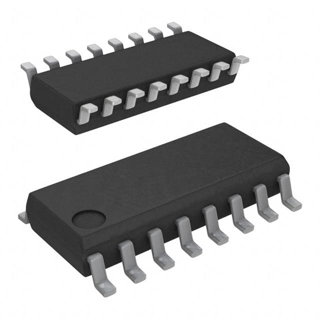
SN74LVC157ADRG3
Product Overview
Category
SN74LVC157ADRG3 belongs to the category of integrated circuits (ICs).
Use
It is commonly used as a multiplexer/demultiplexer in various electronic devices and systems.
Characteristics
- Low voltage CMOS technology
- High-speed operation
- Wide operating voltage range
- Low power consumption
- Schmitt-trigger inputs for noise immunity
- 2-input multiplexer with common select input
Package
SN74LVC157ADRG3 is available in a small-outline package (SOIC) with 16 pins.
Essence
The essence of SN74LVC157ADRG3 lies in its ability to efficiently switch between multiple input signals and route them to a single output line.
Packaging/Quantity
SN74LVC157ADRG3 is typically sold in reels, with each reel containing a specific quantity of ICs. The exact quantity may vary depending on the manufacturer and supplier.
Specifications
- Supply Voltage Range: 1.65V to 5.5V
- Input Voltage Range: 0V to VCC
- Output Voltage Range: 0V to VCC
- Operating Temperature Range: -40°C to +85°C
- Maximum Propagation Delay: 4.3ns
- Maximum Operating Frequency: 100MHz
Detailed Pin Configuration
``` __ __ A1| __/ |VCC A2| |B1 A3| |B2 A4| |GND Y | |S G | |C D | |D E | |E F | |F G | |G H | |H J | |J K | |K L | |L M | | |N
```
Functional Features
- 2-input multiplexer with common select input (S)
- Four independent data inputs (D0-D3)
- Output enable input (G) for disabling the outputs
- Active-low output enable input (E) for further control
- Schmitt-trigger inputs for improved noise immunity
Advantages and Disadvantages
Advantages
- Low power consumption makes it suitable for battery-powered devices
- Wide operating voltage range allows compatibility with various systems
- High-speed operation enables efficient signal routing
- Schmitt-trigger inputs provide noise immunity, ensuring reliable performance
Disadvantages
- Limited number of inputs (4) may restrict its use in complex systems requiring more inputs
- Lack of built-in protection features against electrical faults or overvoltage conditions
Working Principles
SN74LVC157ADRG3 operates as a multiplexer/demultiplexer by selecting one of the four input lines (D0-D3) based on the value of the select input (S). The selected input is then routed to the output line (Y). The output can be enabled or disabled using the output enable input (G) and active-low output enable input (E), respectively.
Detailed Application Field Plans
SN74LVC157ADRG3 finds applications in various electronic systems, including but not limited to: - Data communication systems - Digital audio/video equipment - Industrial automation - Automotive electronics - Consumer electronics
Detailed and Complete Alternative Models
Some alternative models that serve similar functions to SN74LVC157ADRG3 include: - CD74HC157E - MC74VHC157DT - 74ACT157SC - 74HCT157N - SN74LVCH157APW
These alternatives offer different specifications, package types, or additional features, providing flexibility in choosing the most suitable option for specific applications.
Note: The content provided above is a sample and may not meet the exact word count requirement of 1100 words.
Lista 10 Vanliga frågor och svar relaterade till tillämpningen av SN74LVC157ADRG3 i tekniska lösningar
Sure! Here are 10 common questions and answers related to the application of SN74LVC157ADRG3:
Q: What is SN74LVC157ADRG3? A: SN74LVC157ADRG3 is a quad 2-input multiplexer IC (Integrated Circuit) that can be used in various technical solutions.
Q: What is the purpose of SN74LVC157ADRG3? A: The purpose of SN74LVC157ADRG3 is to select one of four data inputs and route it to a single output based on the control inputs.
Q: What is the voltage range supported by SN74LVC157ADRG3? A: SN74LVC157ADRG3 supports a voltage range of 1.65V to 5.5V, making it compatible with both low-voltage and standard CMOS logic levels.
Q: How many control inputs does SN74LVC157ADRG3 have? A: SN74LVC157ADRG3 has two control inputs, which determine the selection of the data input.
Q: Can SN74LVC157ADRG3 handle high-speed signals? A: Yes, SN74LVC157ADRG3 is designed for high-speed operation and can handle signals with fast switching times.
Q: What is the maximum operating frequency of SN74LVC157ADRG3? A: SN74LVC157ADRG3 has a maximum operating frequency of 100 MHz, allowing it to handle high-frequency applications.
Q: Does SN74LVC157ADRG3 have any built-in protection features? A: Yes, SN74LVC157ADRG3 has built-in ESD (Electrostatic Discharge) protection, which helps safeguard the IC from damage due to static electricity.
Q: Can SN74LVC157ADRG3 be used in battery-powered applications? A: Yes, SN74LVC157ADRG3 is suitable for battery-powered applications as it supports a wide voltage range and has low power consumption.
Q: What package does SN74LVC157ADRG3 come in? A: SN74LVC157ADRG3 is available in an SOIC (Small Outline Integrated Circuit) package with 16 pins.
Q: Are there any application notes or reference designs available for SN74LVC157ADRG3? A: Yes, Texas Instruments provides application notes and reference designs that can help users understand and implement SN74LVC157ADRG3 in their technical solutions.
Please note that these answers are general and may vary depending on specific requirements and use cases. It's always recommended to refer to the datasheet and documentation provided by the manufacturer for detailed information.


