

SN74LVC1G07YEAR
Product Overview
- Category: Integrated Circuit (IC)
- Use: Logic Gate Buffer/Driver
- Characteristics: Low-Voltage CMOS, Single Buffer/Driver
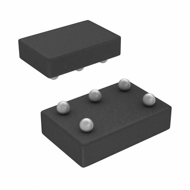
- Package: SOT-23-5
- Essence: Single Buffer/Driver with Open-Drain Output
- Packaging/Quantity: Tape and Reel, 3000 pieces per reel
Specifications
- Supply Voltage Range: 1.65V to 5.5V
- Input Voltage Range: 0V to VCC
- Output Voltage Range: 0V to VCC
- Maximum Operating Frequency: 100 MHz
- Propagation Delay: 3.8 ns (typical)
- Output Drive Capability: ±24 mA
- Operating Temperature Range: -40°C to +85°C
Detailed Pin Configuration
The SN74LVC1G07YEAR has a total of 5 pins:
- GND: Ground pin
- IN: Input pin for the logic signal
- OUT: Output pin for the buffered logic signal
- VCC: Positive power supply pin
- NC: No connection pin (not internally connected)
Functional Features
- Single buffer/driver with open-drain output
- Provides buffering and level shifting capabilities
- Supports bidirectional communication
- Allows multiple devices to share a common bus line
- High-speed operation with low power consumption
- Compatible with various logic families
Advantages and Disadvantages
Advantages: - Small package size allows for space-saving designs - Wide operating voltage range enables compatibility with different systems - Low propagation delay ensures fast signal transmission - Open-drain output provides flexibility in connecting to other devices - High output drive capability allows for driving capacitive loads
Disadvantages: - Limited number of buffer/driver channels (only one in this case) - Open-drain output requires external pull-up resistor for proper operation - Not suitable for applications requiring high-speed data transfer
Working Principles
The SN74LVC1G07YEAR is a single buffer/driver IC that operates on low-voltage CMOS technology. It takes an input logic signal and buffers it to provide a level-shifted output signal. The open-drain output allows the device to be connected to other devices or systems, enabling bidirectional communication.
The IC operates within a wide supply voltage range, making it compatible with various systems. It has a fast propagation delay, ensuring quick signal transmission. The high output drive capability allows it to drive capacitive loads without significant degradation in performance.
To ensure proper operation, an external pull-up resistor is required to pull the output signal to the desired logic level when the output is in the high-impedance state.
Detailed Application Field Plans
The SN74LVC1G07YEAR can be used in various applications, including:
- Communication Systems: It can be used as a level shifter in serial communication interfaces such as I2C, SPI, or UART.
- Sensor Networks: It can interface sensors with different voltage levels to microcontrollers or processors.
- Industrial Control Systems: It can be used in control circuits for driving relays, solenoids, or LEDs.
- Automotive Electronics: It can be utilized in automotive systems for level shifting and buffering signals between different components.
- Battery-Powered Devices: Its low power consumption makes it suitable for portable devices operating on battery power.
Detailed and Complete Alternative Models
Some alternative models to the SN74LVC1G07YEAR are:
- SN74LVC1G07DBVR: SOT-23-5 package, same functionality as SN74LVC1G07YEAR.
- NC7SZ07P5X: SC-70 package, single buffer/driver with open-drain output.
- 74LVC1G07GW: SOT-353 package, low-voltage CMOS buffer/driver with open-drain output.
These alternative models offer similar functionality and can be used as replacements depending on specific requirements and availability.
Word count: 511 words
Lista 10 Vanliga frågor och svar relaterade till tillämpningen av SN74LVC1G07YEAR i tekniska lösningar
Sure! Here are 10 common questions and answers related to the application of SN74LVC1G07YEAR in technical solutions:
Q1: What is SN74LVC1G07YEAR? A1: SN74LVC1G07YEAR is a single buffer/driver with open-drain output, designed for voltage level translation.
Q2: What is the operating voltage range of SN74LVC1G07YEAR? A2: The operating voltage range is from 1.65V to 5.5V.
Q3: What is the maximum output current of SN74LVC1G07YEAR? A3: The maximum output current is typically 32mA.
Q4: Can SN74LVC1G07YEAR be used as a level shifter? A4: Yes, SN74LVC1G07YEAR can be used as a level shifter to convert signals between different voltage levels.
Q5: What is the maximum data rate supported by SN74LVC1G07YEAR? A5: SN74LVC1G07YEAR supports a maximum data rate of up to 100 Mbps.
Q6: Is SN74LVC1G07YEAR suitable for bidirectional communication? A6: No, SN74LVC1G07YEAR is a unidirectional buffer/driver and not suitable for bidirectional communication.
Q7: Can SN74LVC1G07YEAR drive capacitive loads? A7: Yes, SN74LVC1G07YEAR can drive capacitive loads up to 50pF.
Q8: Does SN74LVC1G07YEAR have built-in protection features? A8: Yes, SN74LVC1G07YEAR has built-in protection against electrostatic discharge (ESD) and latch-up.
Q9: What is the package type of SN74LVC1G07YEAR? A9: SN74LVC1G07YEAR is available in a small SOT-23-5 package.
Q10: Can SN74LVC1G07YEAR be used in automotive applications? A10: Yes, SN74LVC1G07YEAR is qualified for automotive applications and meets the AEC-Q100 standard.
Please note that these answers are general and may vary depending on the specific datasheet and application requirements.