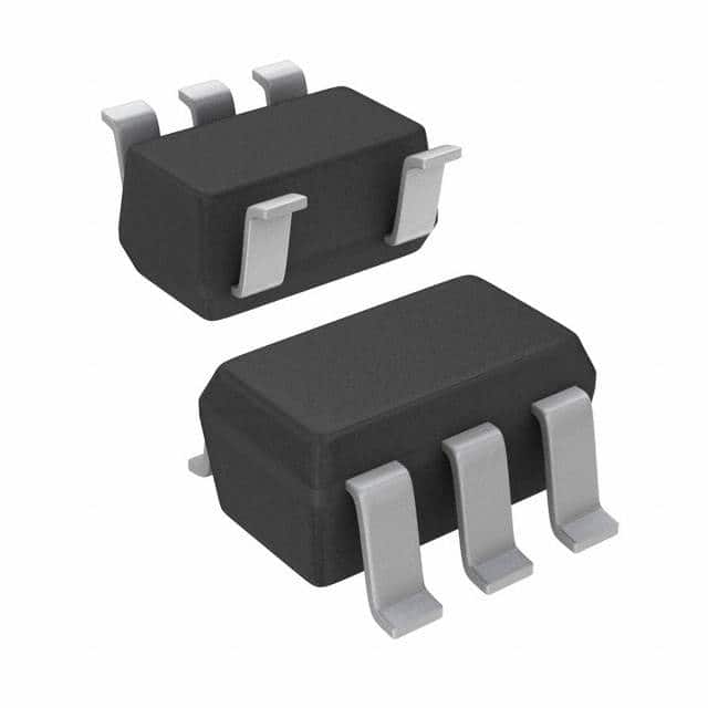
SN74LVC1G17DBVTE4
Product Overview
- Category: Integrated Circuit (IC)
- Use: Logic Gate
- Characteristics: Single Schmitt-Trigger Buffer/Driver
- Package: SOT-23 (DBV) package
- Essence: High-speed CMOS technology
- Packaging/Quantity: Tape and Reel, 3000 pieces per reel
Specifications
- Supply Voltage Range: 1.65V to 5.5V
- Input Voltage Range: 0V to VCC
- Output Voltage Range: 0V to VCC
- Maximum Operating Frequency: 400 MHz
- Propagation Delay: 3.8 ns (typical)
- Low Power Consumption: ICC = 2 µA (maximum)
Detailed Pin Configuration
The SN74LVC1G17DBVTE4 has the following pin configuration:
____
   A1 |    | VCC
   A2 |    | Y
   GND |____|
Functional Features
- Single Schmitt-trigger buffer/driver with open-drain output
- Converts slowly changing input signals into sharply defined, jitter-free output signals
- Provides hysteresis for improved noise immunity
- Allows direct interface with different logic levels
- Supports bidirectional voltage translation
Advantages
- High-speed operation enables efficient signal processing
- Wide supply voltage range allows compatibility with various systems
- Low power consumption reduces energy usage
- Small package size saves board space
- Open-drain output provides flexibility in circuit design
Disadvantages
- Limited output current capability
- Not suitable for high-power applications
- Requires external pull-up resistor for proper operation
Working Principles
The SN74LVC1G17DBVTE4 is a single Schmitt-trigger buffer/driver that converts slowly changing input signals into sharply defined, jitter-free output signals. It utilizes high-speed CMOS technology to achieve fast operation and low power consumption. The device incorporates hysteresis, which improves noise immunity by providing a threshold voltage range for input signal detection.
The open-drain output allows bidirectional voltage translation and direct interface with different logic levels. However, an external pull-up resistor is required to provide the necessary current when driving high logic levels.
Detailed Application Field Plans
The SN74LVC1G17DBVTE4 is commonly used in various applications, including:
- Communication Systems: Signal buffering and level shifting in data transmission circuits.
- Industrial Automation: Interface between different logic levels in control systems.
- Consumer Electronics: Voltage translation in portable devices and audio/video equipment.
- Automotive Electronics: Signal conditioning and level conversion in automotive control modules.
- Internet of Things (IoT): Logic level adaptation in IoT sensor nodes and edge devices.
Detailed and Complete Alternative Models
- SN74LVC1G07DBVR: Single Buffer/Driver with Open-Drain Output
- SN74LVC1G14DBVR: Single Schmitt-Trigger Inverter with Open-Drain Output
- SN74LVC1G125DBVR: Single Bus Buffer Gate with 3-State Output
These alternative models offer similar functionality and can be considered as replacements for the SN74LVC1G17DBVTE4 in different applications.
Word count: 410 words
Lista 10 Vanliga frågor och svar relaterade till tillämpningen av SN74LVC1G17DBVTE4 i tekniska lösningar
Sure! Here are 10 common questions and answers related to the application of SN74LVC1G17DBVTE4 in technical solutions:
Q1: What is SN74LVC1G17DBVTE4? A1: SN74LVC1G17DBVTE4 is a single Schmitt-trigger buffer/driver with a standard push-pull output. It is commonly used in digital logic applications.
Q2: What is the voltage supply range for SN74LVC1G17DBVTE4? A2: The voltage supply range for SN74LVC1G17DBVTE4 is typically between 1.65V and 5.5V.
Q3: What is the maximum output current of SN74LVC1G17DBVTE4? A3: The maximum output current of SN74LVC1G17DBVTE4 is 32mA.
Q4: Can SN74LVC1G17DBVTE4 be used as a level shifter? A4: Yes, SN74LVC1G17DBVTE4 can be used as a level shifter to convert signals between different voltage levels.
Q5: What is the input threshold voltage of SN74LVC1G17DBVTE4? A5: The input threshold voltage of SN74LVC1G17DBVTE4 is typically 0.8V.
Q6: Is SN74LVC1G17DBVTE4 compatible with both CMOS and TTL logic levels? A6: Yes, SN74LVC1G17DBVTE4 is compatible with both CMOS (Complementary Metal-Oxide-Semiconductor) and TTL (Transistor-Transistor Logic) logic levels.
Q7: Can SN74LVC1G17DBVTE4 be used in high-speed applications? A7: Yes, SN74LVC1G17DBVTE4 is designed for high-speed operation and can be used in applications with fast switching requirements.
Q8: What is the propagation delay of SN74LVC1G17DBVTE4? A8: The propagation delay of SN74LVC1G17DBVTE4 is typically around 3.5ns.
Q9: Can SN74LVC1G17DBVTE4 drive capacitive loads? A9: Yes, SN74LVC1G17DBVTE4 can drive capacitive loads up to a certain limit specified in the datasheet.
Q10: Is SN74LVC1G17DBVTE4 available in different package options? A10: Yes, SN74LVC1G17DBVTE4 is available in various package options, including SOT-23 and VSSOP, to suit different application requirements.
Please note that the answers provided here are general and may vary depending on specific datasheet specifications and application conditions.


