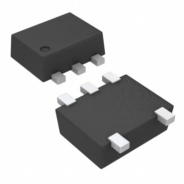
SN74LVC1G17DRLRG4
Product Overview
- Category: Integrated Circuit (IC)
- Use: Logic Gate
- Characteristics: Single Schmitt-Trigger Buffer/Driver
- Package: SOT-553
- Essence: High-speed CMOS technology
- Packaging/Quantity: Tape and Reel, 3000 pieces per reel
Specifications
- Supply Voltage Range: 1.65V to 5.5V
- Input Voltage Range: 0V to VCC
- Output Voltage Range: 0V to VCC
- Operating Temperature Range: -40°C to +125°C
- Propagation Delay: 3.8ns (typical) at 3.3V
- Output Drive Capability: ±24mA at 3.3V
Detailed Pin Configuration
The SN74LVC1G17DRLRG4 has the following pin configuration:
____
   A1 |    | VCC
   A2 |    | Y
  GND |____| A
Functional Features
- Single Schmitt-trigger buffer/driver with open-drain output
- Provides signal conditioning and level shifting capabilities
- Suitable for interfacing between different logic families
- Wide supply voltage range allows compatibility with various systems
- High-speed operation enables efficient data transmission
Advantages and Disadvantages
Advantages
- Compact size and low power consumption
- High noise immunity due to Schmitt-trigger input
- Open-drain output allows easy connection to other devices
- Wide operating temperature range for versatile applications
Disadvantages
- Limited output drive capability compared to some other ICs
- Not suitable for high-voltage applications
Working Principles
The SN74LVC1G17DRLRG4 is a single Schmitt-trigger buffer/driver IC. It operates by receiving an input signal (A) and providing a conditioned output signal (Y). The Schmitt-trigger input ensures noise immunity and hysteresis, making it suitable for applications with varying input voltages. The open-drain output allows easy connection to other devices, enabling bidirectional communication.
Detailed Application Field Plans
The SN74LVC1G17DRLRG4 can be used in various applications, including:
- Level shifting: It can be used to convert logic levels between different voltage domains, allowing seamless communication between incompatible systems.
- Signal conditioning: The Schmitt-trigger input helps clean up noisy signals, making it useful in applications where reliable data transmission is crucial.
- Interface buffering: It can act as a buffer between a microcontroller and other peripheral devices, ensuring proper signal integrity and preventing damage to sensitive components.
Detailed and Complete Alternative Models
- SN74LVC1G17DBVR
- SN74LVC1G17DCKR
- SN74LVC1G17DRLR
These alternative models offer similar functionality and characteristics, providing flexibility in choosing the most suitable option for specific applications.
Word count: 346 words
Lista 10 Vanliga frågor och svar relaterade till tillämpningen av SN74LVC1G17DRLRG4 i tekniska lösningar
Sure! Here are 10 common questions and answers related to the application of SN74LVC1G17DRLRG4 in technical solutions:
Q1: What is SN74LVC1G17DRLRG4? A1: SN74LVC1G17DRLRG4 is a single Schmitt-trigger buffer/driver with open-drain output, commonly used in digital logic applications.
Q2: What is the voltage supply range for SN74LVC1G17DRLRG4? A2: The voltage supply range for SN74LVC1G17DRLRG4 is typically between 1.65V and 5.5V.
Q3: What is the maximum output current of SN74LVC1G17DRLRG4? A3: The maximum output current of SN74LVC1G17DRLRG4 is typically 32mA.
Q4: Can SN74LVC1G17DRLRG4 be used as a level shifter? A4: Yes, SN74LVC1G17DRLRG4 can be used as a level shifter to convert signals between different voltage levels.
Q5: What is the input threshold voltage of SN74LVC1G17DRLRG4? A5: The input threshold voltage of SN74LVC1G17DRLRG4 is typically 0.8V.
Q6: Is SN74LVC1G17DRLRG4 suitable for high-speed applications? A6: Yes, SN74LVC1G17DRLRG4 is designed for high-speed operation and can be used in applications with fast switching requirements.
Q7: Can SN74LVC1G17DRLRG4 drive capacitive loads? A7: Yes, SN74LVC1G17DRLRG4 can drive small capacitive loads, but it is recommended to add a series resistor to limit the current during charging and discharging.
Q8: What is the maximum propagation delay of SN74LVC1G17DRLRG4? A8: The maximum propagation delay of SN74LVC1G17DRLRG4 is typically 5.2ns.
Q9: Can SN74LVC1G17DRLRG4 be used in battery-powered applications? A9: Yes, SN74LVC1G17DRLRG4 has a low power consumption and can be used in battery-powered applications.
Q10: Is SN74LVC1G17DRLRG4 available in different package options? A10: Yes, SN74LVC1G17DRLRG4 is available in various package options, including SOT-23 and X2SON.


