

SN74LVC1G18YZAR
Product Overview
- Category: Integrated Circuit
- Use: Logic Gate
- Characteristics: Single Schmitt-Trigger Buffer
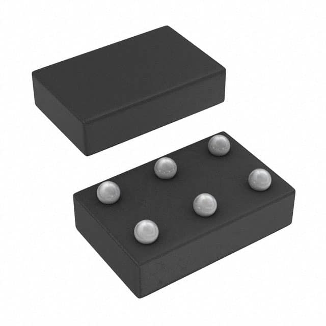
- Package: SOT-23-5
- Essence: High-speed CMOS technology
- Packaging/Quantity: Tape and Reel, 3000 pieces per reel
Specifications
- Supply Voltage Range: 1.65V to 5.5V
- Input Voltage Range: -0.5V to VCC + 0.5V
- Output Voltage Range: 0V to VCC
- Maximum Operating Frequency: 100 MHz
- Propagation Delay: 3.8 ns (typical)
- Low Power Consumption: ICC = 2 µA (maximum)
Detailed Pin Configuration
The SN74LVC1G18YZAR has a total of 5 pins:
- GND (Ground): Connected to the ground reference potential.
- A (Input): Input pin for the logic signal.
- Y (Output): Output pin for the logic signal.
- VCC (Power): Connected to the positive supply voltage.
- NC (Not Connected): This pin is not connected internally and can be left unconnected.
Functional Features
- Single Schmitt-Trigger Buffer: Converts input signals with slow transition times into clean digital outputs.
- High-Speed CMOS Technology: Provides fast switching speeds and low power consumption.
- Wide Supply Voltage Range: Allows compatibility with various systems.
- Small Package Size: SOT-23-5 package enables space-saving designs.
- Low Propagation Delay: Ensures minimal delay in signal transmission.
Advantages and Disadvantages
Advantages: - High-speed operation allows for efficient signal processing. - Low power consumption reduces energy requirements. - Wide supply voltage range enhances compatibility. - Small package size facilitates compact circuit designs.
Disadvantages: - Limited functionality as a single Schmitt-trigger buffer. - Not suitable for applications requiring complex logic operations.
Working Principles
The SN74LVC1G18YZAR is a single Schmitt-trigger buffer that operates based on high-speed CMOS technology. It receives an input signal (A) and converts it into a clean digital output signal (Y). The Schmitt-trigger feature ensures that the output transitions occur at different voltage levels for rising and falling input signals, providing noise immunity and hysteresis.
Detailed Application Field Plans
The SN74LVC1G18YZAR finds application in various fields, including:
- Consumer Electronics: Used in smartphones, tablets, and portable devices for signal conditioning and level shifting.
- Industrial Automation: Employed in control systems, sensors, and actuators for reliable signal processing.
- Automotive Electronics: Integrated into automotive modules for signal buffering and voltage level conversion.
- Communication Systems: Utilized in networking equipment and data transmission circuits for signal integrity enhancement.
Detailed and Complete Alternative Models
- SN74LVC1G17DBVR: Single Schmitt-Trigger Buffer with Open-Drain Output, SOT-23-5 package.
- SN74LVC1G07DCKR: Single Buffer/Driver with Open-Drain Output, SC-70-5 package.
- SN74LVC1G04DCKR: Single Inverter Gate, SC-70-5 package.
- SN74LVC1G08DCKR: Single 2-Input AND Gate, SC-70-5 package.
- SN74LVC1G86DCKR: Single 2-Input Exclusive-OR Gate, SC-70-5 package.
These alternative models offer similar functionality and can be used as substitutes depending on specific design requirements.
Word count: 399 words
Lista 10 Vanliga frågor och svar relaterade till tillämpningen av SN74LVC1G18YZAR i tekniska lösningar
Sure! Here are 10 common questions and answers related to the application of SN74LVC1G18YZAR:
1. What is SN74LVC1G18YZAR? - SN74LVC1G18YZAR is a single-gate buffer/driver with open-drain output, which is commonly used in digital logic circuits.
2. What is the voltage supply range for SN74LVC1G18YZAR? - The voltage supply range for SN74LVC1G18YZAR is typically between 1.65V and 5.5V.
3. What is the maximum output current of SN74LVC1G18YZAR? - The maximum output current of SN74LVC1G18YZAR is typically 32mA.
4. Can SN74LVC1G18YZAR be used as a level shifter? - Yes, SN74LVC1G18YZAR can be used as a level shifter to convert signals from one voltage level to another.
5. What is the propagation delay of SN74LVC1G18YZAR? - The propagation delay of SN74LVC1G18YZAR is typically around 4.6ns.
6. Is SN74LVC1G18YZAR suitable for high-speed applications? - Yes, SN74LVC1G18YZAR is designed for high-speed operation and can be used in various high-speed applications.
7. Can SN74LVC1G18YZAR drive capacitive loads? - Yes, SN74LVC1G18YZAR can drive small capacitive loads without any additional buffering.
8. Does SN74LVC1G18YZAR have built-in protection features? - Yes, SN74LVC1G18YZAR has built-in protection features like overvoltage and undervoltage lockout.
9. Can SN74LVC1G18YZAR be used in battery-powered applications? - Yes, SN74LVC1G18YZAR is suitable for battery-powered applications due to its low power consumption.
10. What is the package type of SN74LVC1G18YZAR? - SN74LVC1G18YZAR is available in a small SOT-23 package, which is commonly used for surface mount applications.
Please note that the answers provided here are general and may vary depending on specific datasheet specifications and application requirements.