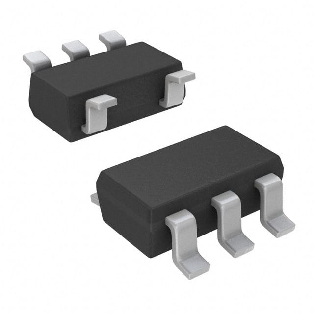
SN74LVC1G34DCKRE4
Product Overview
- Category: Integrated Circuit (IC)
- Use: Logic Gate
- Characteristics: Single Buffer/Driver, Non-Inverting, 3-State Output
- Package: SC-70 (6-Pin), Tape and Reel
- Essence: High-Speed CMOS Logic
- Packaging/Quantity: 2500 units per reel
Specifications
- Supply Voltage Range: 1.65V to 5.5V
- Input Voltage Range: -0.5V to VCC + 0.5V
- Output Voltage Range: 0V to VCC
- Maximum Input Current: ±20mA
- Maximum Output Current: ±32mA
- Propagation Delay: 2.9ns (typical)
- Operating Temperature Range: -40°C to 85°C
Detailed Pin Configuration
The SN74LVC1G34DCKRE4 has a total of 6 pins:
- GND (Ground)
- A (Input)
- Y (Output)
- OE (Output Enable)
- NC (No Connection)
- VCC (Power Supply)
Functional Features
- Single non-inverting buffer/driver with 3-state output
- High-speed operation suitable for various applications
- Supports mixed-mode signal operation on all ports
- Low power consumption
- Schmitt-trigger input allows for slow input transition and noise immunity
Advantages
- Compact size and low pin count make it ideal for space-constrained designs
- Wide supply voltage range allows for compatibility with different systems
- 3-state output enables easy bus sharing and reduces conflicts
- High-speed operation enhances overall system performance
- Schmitt-trigger input ensures reliable operation in noisy environments
Disadvantages
- Limited output current may not be suitable for driving heavy loads
- Single buffer/driver limits the number of outputs that can be controlled independently
Working Principles
The SN74LVC1G34DCKRE4 is a single non-inverting buffer/driver IC. It takes an input signal and amplifies it to drive an output signal. The 3-state output allows the device to be effectively disconnected from the bus when not in use, reducing conflicts and enabling easy bus sharing.
The Schmitt-trigger input ensures reliable operation by providing hysteresis, allowing for slow input transitions and noise immunity. The IC operates at high speeds, making it suitable for various applications where fast signal propagation is required.
Detailed Application Field Plans
The SN74LVC1G34DCKRE4 finds applications in a wide range of fields, including:
- Consumer Electronics: Used in smartphones, tablets, and portable devices for signal buffering and level shifting.
- Automotive: Employed in automotive electronics for signal conditioning and interfacing between different voltage domains.
- Industrial Automation: Utilized in control systems, sensors, and actuators for signal amplification and isolation.
- Communication Systems: Integrated into networking equipment, routers, and switches for signal buffering and line driving.
- Medical Devices: Incorporated in medical instruments and diagnostic equipment for signal processing and amplification.
Detailed and Complete Alternative Models
- SN74LVC1G34DBVR: SOT-23 (5-Pin) package, tape and reel packaging, 3000 units per reel.
- SN74LVC1G34YZPR: DSBGA (4-Ball) package, tape and reel packaging, 4000 units per reel.
- SN74LVC1G34DRLR: X2SON (6-Pin) package, tape and reel packaging, 2500 units per reel.
These alternative models offer similar functionality and characteristics to the SN74LVC1G34DCKRE4, providing flexibility in choosing the most suitable option for specific design requirements.
Word count: 511 words
Lista 10 Vanliga frågor och svar relaterade till tillämpningen av SN74LVC1G34DCKRE4 i tekniska lösningar
Sure! Here are 10 common questions and answers related to the application of SN74LVC1G34DCKRE4 in technical solutions:
1. What is SN74LVC1G34DCKRE4? - SN74LVC1G34DCKRE4 is a single buffer gate IC (Integrated Circuit) that provides high-speed signal buffering in digital circuits.
2. What is the voltage range supported by SN74LVC1G34DCKRE4? - SN74LVC1G34DCKRE4 supports a wide voltage range from 1.65V to 5.5V, making it compatible with various logic families.
3. What is the maximum output current of SN74LVC1G34DCKRE4? - The maximum output current of SN74LVC1G34DCKRE4 is typically 32mA, allowing it to drive multiple loads.
4. Can SN74LVC1G34DCKRE4 be used as a level shifter? - Yes, SN74LVC1G34DCKRE4 can be used as a level shifter to convert signals between different voltage levels.
5. Is SN74LVC1G34DCKRE4 suitable for bidirectional communication? - No, SN74LVC1G34DCKRE4 is a unidirectional buffer gate and does not support bidirectional communication.
6. What is the propagation delay of SN74LVC1G34DCKRE4? - The propagation delay of SN74LVC1G34DCKRE4 is typically around 4.3ns, making it suitable for high-speed applications.
7. Can SN74LVC1G34DCKRE4 be used in battery-powered devices? - Yes, SN74LVC1G34DCKRE4 is designed to operate at low power and can be used in battery-powered devices.
8. Does SN74LVC1G34DCKRE4 have built-in ESD protection? - Yes, SN74LVC1G34DCKRE4 has built-in ESD (Electrostatic Discharge) protection, ensuring robustness against static electricity.
9. Can SN74LVC1G34DCKRE4 drive capacitive loads? - Yes, SN74LVC1G34DCKRE4 can drive capacitive loads up to a certain limit, typically around 50pF.
10. Is SN74LVC1G34DCKRE4 available in different package options? - Yes, SN74LVC1G34DCKRE4 is available in various package options, including SOT-23 and SC-70, providing flexibility in design and layout considerations.
Please note that the answers provided here are general and may vary depending on specific datasheet specifications and application requirements.


