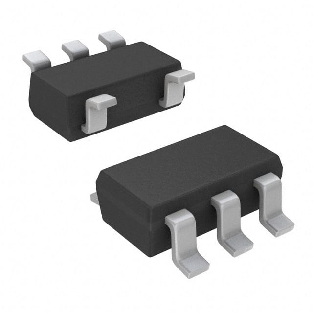
SN74LVC1G86QDCKTQ1
Product Overview
Category
The SN74LVC1G86QDCKTQ1 belongs to the category of integrated circuits (ICs).
Use
This IC is commonly used for signal processing and logic functions in various electronic devices.
Characteristics
- Low-voltage CMOS technology
- Single 2-input XOR gate
- High-speed operation
- Wide operating voltage range: 1.65V to 5.5V
- Low power consumption
- Schmitt-trigger input for noise immunity
- Small package size for space-constrained applications
Package
The SN74LVC1G86QDCKTQ1 is available in a small SOT-353 package.
Essence
The essence of this IC lies in its ability to perform XOR logic operations efficiently and reliably.
Packaging/Quantity
The SN74LVC1G86QDCKTQ1 is typically packaged in reels, with each reel containing a specific quantity of ICs. The exact quantity may vary depending on the manufacturer's specifications.
Specifications
- Supply Voltage Range: 1.65V to 5.5V
- Input Voltage Range: 0V to VCC
- Output Voltage Range: 0V to VCC
- Operating Temperature Range: -40°C to +125°C
- Propagation Delay: 3.8ns (typical)
- Maximum Quiescent Current: 10μA
- Maximum Output Current: ±32mA
Detailed Pin Configuration
The SN74LVC1G86QDCKTQ1 has the following pin configuration:
____
   A --|    |-- VCC
   B --|    |-- Y
 GND --|____|-- NC
- A: Input A
- B: Input B
- VCC: Power supply voltage
- Y: Output
- GND: Ground
- NC: No connection
Functional Features
The SN74LVC1G86QDCKTQ1 is a single 2-input XOR gate. It performs the exclusive OR logic operation on its two input signals (A and B) and provides the result at the output pin (Y). The IC operates at high speed, making it suitable for applications that require fast signal processing. It also incorporates a Schmitt-trigger input, which enhances noise immunity and ensures reliable operation in noisy environments.
Advantages and Disadvantages
Advantages
- Low power consumption
- Wide operating voltage range
- Small package size for space-constrained applications
- High-speed operation
- Schmitt-trigger input for noise immunity
Disadvantages
- Limited to XOR logic operation only
- Single gate functionality may not be suitable for complex logic circuits
Working Principles
The SN74LVC1G86QDCKTQ1 operates based on the principles of CMOS technology. It utilizes complementary metal-oxide-semiconductor transistors to perform the XOR logic operation. When both inputs (A and B) are different, the output (Y) will be high. Conversely, when both inputs are the same, the output will be low. The Schmitt-trigger input helps to eliminate noise and ensure stable logic levels.
Detailed Application Field Plans
The SN74LVC1G86QDCKTQ1 finds applications in various electronic devices and systems, including but not limited to: - Consumer electronics - Mobile devices - Automotive electronics - Industrial automation - Communication systems - Medical equipment
Its compact size, low power consumption, and high-speed operation make it suitable for space-constrained applications where efficient signal processing and logic functions are required.
Detailed and Complete Alternative Models
Some alternative models that offer similar functionality to the SN74LVC1G86QDCKTQ1 include: - 74LVC1G86GW,125 - MC74VHC1G86DTT1G - TC7SZ86FU
These alternatives can be considered based on specific requirements such as package type, voltage range, or additional features.
In conclusion, the SN74LVC1G86QDCKTQ1 is a versatile integrated circuit that provides efficient XOR logic operations. Its low power consumption, wide operating voltage range, and small package size make it suitable for various applications in different industries. However, its single gate functionality may limit its use in complex logic circuits.
Lista 10 Vanliga frågor och svar relaterade till tillämpningen av SN74LVC1G86QDCKTQ1 i tekniska lösningar
Sure! Here are 10 common questions and answers related to the application of SN74LVC1G86QDCKTQ1 in technical solutions:
1. What is SN74LVC1G86QDCKTQ1? SN74LVC1G86QDCKTQ1 is a single 2-input XOR gate IC (integrated circuit) that is commonly used in digital logic circuits.
2. What is the operating voltage range for SN74LVC1G86QDCKTQ1? The operating voltage range for SN74LVC1G86QDCKTQ1 is typically between 1.65V and 5.5V.
3. What is the maximum output current of SN74LVC1G86QDCKTQ1? The maximum output current of SN74LVC1G86QDCKTQ1 is around 32mA.
4. Can SN74LVC1G86QDCKTQ1 be used in battery-powered applications? Yes, SN74LVC1G86QDCKTQ1 can be used in battery-powered applications as it operates at low voltages and has low power consumption.
5. What is the propagation delay of SN74LVC1G86QDCKTQ1? The propagation delay of SN74LVC1G86QDCKTQ1 is typically around 3.8ns.
6. Can SN74LVC1G86QDCKTQ1 be used in high-speed applications? Yes, SN74LVC1G86QDCKTQ1 can be used in high-speed applications as it has a fast switching speed.
7. Is SN74LVC1G86QDCKTQ1 compatible with other logic families? Yes, SN74LVC1G86QDCKTQ1 is compatible with a wide range of logic families, including TTL and CMOS.
8. Can SN74LVC1G86QDCKTQ1 be used in automotive applications? Yes, SN74LVC1G86QDCKTQ1 is specifically designed for automotive applications and is qualified to meet automotive industry standards.
9. What is the package type for SN74LVC1G86QDCKTQ1? SN74LVC1G86QDCKTQ1 is available in a small SOT-353 package.
10. Where can I find more information about the application of SN74LVC1G86QDCKTQ1? You can find more detailed information about the application of SN74LVC1G86QDCKTQ1 in the datasheet provided by the manufacturer or by referring to technical resources and application notes available online.


