

SN74LVC1GU04YZTR
Product Overview
Category
SN74LVC1GU04YZTR belongs to the category of integrated circuits (ICs).
Use
This product is commonly used as an inverter, which means it can convert a logic level from high to low or vice versa.
Characteristics
- Low voltage operation: This IC operates at a low voltage range, typically between 1.65V and 5.5V.
- High-speed performance: It offers fast switching speeds, making it suitable for applications that require quick response times.
- Low power consumption: The SN74LVC1GU04YZTR is designed to consume minimal power, making it energy-efficient.
- Small package size: It comes in a small form factor, allowing for space-saving designs.
- RoHS compliant: This product meets the Restriction of Hazardous Substances directive, ensuring its environmental friendliness.
Package
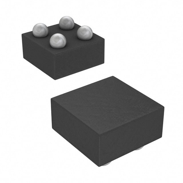
The SN74LVC1GU04YZTR is available in a small-outline transistor (SOT) package.
Essence
The essence of this product lies in its ability to perform logic level inversion, enabling signal processing and control in various electronic systems.
Packaging/Quantity
This IC is typically packaged in reels, with each reel containing a specific quantity of units. The exact quantity may vary depending on the manufacturer's specifications.
Specifications
- Supply Voltage Range: 1.65V to 5.5V
- Input Voltage Range: 0V to VCC
- Output Voltage Range: 0V to VCC
- Operating Temperature Range: -40°C to +85°C
- Maximum Propagation Delay: 4.3 ns (at 3.3V)
- Maximum Quiescent Current: 10 µA (at 5.5V)
Detailed Pin Configuration
The SN74LVC1GU04YZTR has the following pin configuration:
____
   VCC|    |GND
  IN A|    |OUT Y
       ----
Functional Features
- Logic level inversion: The SN74LVC1GU04YZTR can invert the logic level of an input signal, providing the complemented output.
- High-speed operation: It offers fast switching speeds, allowing for efficient signal processing.
- Wide voltage range: This IC can operate within a wide voltage range, making it compatible with various systems.
- Low power consumption: It consumes minimal power, reducing energy requirements.
Advantages and Disadvantages
Advantages
- Small package size enables space-saving designs.
- Low power consumption makes it energy-efficient.
- RoHS compliant, ensuring environmental friendliness.
- Wide operating voltage range allows for compatibility with different systems.
Disadvantages
- Limited functionality as it only performs logic level inversion.
- May not be suitable for applications requiring complex logic operations.
Working Principles
The SN74LVC1GU04YZTR works based on the principles of complementary metal-oxide-semiconductor (CMOS) technology. It utilizes a combination of NMOS and PMOS transistors to achieve logic level inversion. When the input voltage is high, the NMOS transistor conducts, pulling the output voltage low. Conversely, when the input voltage is low, the PMOS transistor conducts, driving the output voltage high.
Detailed Application Field Plans
The SN74LVC1GU04YZTR finds applications in various electronic systems, including but not limited to: - Digital logic circuits - Microcontrollers - Data communication systems - Consumer electronics - Automotive electronics
Detailed and Complete Alternative Models
Some alternative models that offer similar functionality to the SN74LVC1GU04YZTR include: - 74HC04: This IC is compatible with a wider voltage range and offers higher noise immunity. - CD4049: It provides multiple inverters in a single package, allowing for more complex logic operations. - NC7SZ04: This IC is designed for ultra-low power applications, making it suitable for battery-powered devices.
Please note that the above alternatives may have different pin configurations and specifications. It is important to refer to their respective datasheets for detailed information.
Word count: 536 words
Lista 10 Vanliga frågor och svar relaterade till tillämpningen av SN74LVC1GU04YZTR i tekniska lösningar
Sure! Here are 10 common questions and answers related to the application of SN74LVC1GU04YZTR in technical solutions:
Q1: What is SN74LVC1GU04YZTR? A1: SN74LVC1GU04YZTR is a single inverter gate IC (integrated circuit) that is commonly used in digital logic applications.
Q2: What is the voltage supply range for SN74LVC1GU04YZTR? A2: The voltage supply range for SN74LVC1GU04YZTR is typically between 1.65V and 5.5V.
Q3: What is the maximum output current of SN74LVC1GU04YZTR? A3: The maximum output current of SN74LVC1GU04YZTR is around 32mA.
Q4: Can SN74LVC1GU04YZTR be used as a level shifter? A4: Yes, SN74LVC1GU04YZTR can be used as a level shifter to convert signals between different voltage levels.
Q5: What is the propagation delay of SN74LVC1GU04YZTR? A5: The propagation delay of SN74LVC1GU04YZTR is typically around 4.3ns.
Q6: Is SN74LVC1GU04YZTR suitable for high-speed applications? A6: Yes, SN74LVC1GU04YZTR is designed for high-speed operation and can be used in various high-frequency applications.
Q7: Can SN74LVC1GU04YZTR be used in battery-powered devices? A7: Yes, SN74LVC1GU04YZTR has a low power consumption and can be used in battery-powered devices.
Q8: Does SN74LVC1GU04YZTR have built-in protection features? A8: Yes, SN74LVC1GU04YZTR has built-in protection features such as overvoltage and undervoltage lockout.
Q9: Can SN74LVC1GU04YZTR be used in automotive applications? A9: Yes, SN74LVC1GU04YZTR is qualified for automotive applications and can withstand harsh operating conditions.
Q10: What is the package type of SN74LVC1GU04YZTR? A10: SN74LVC1GU04YZTR is available in a small SOT-23 package, which is suitable for space-constrained designs.
Please note that these answers are general and may vary depending on specific datasheet specifications and application requirements.