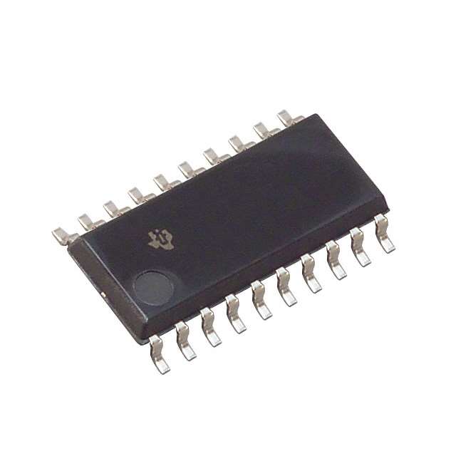
SN74LVC244ANSRE4
Product Overview
Category
SN74LVC244ANSRE4 belongs to the category of integrated circuits (ICs).
Use
It is commonly used as a buffer or line driver in various electronic applications.
Characteristics
- Low-voltage CMOS technology
- High-speed operation
- Wide operating voltage range
- Schmitt-trigger inputs for noise immunity
- 3-state outputs for bus-oriented applications
Package
SN74LVC244ANSRE4 is available in a small-outline package (SOIC) with 20 pins.
Essence
The essence of SN74LVC244ANSRE4 lies in its ability to provide buffering and signal amplification functions in electronic circuits.
Packaging/Quantity
SN74LVC244ANSRE4 is typically packaged in reels, with each reel containing a specific quantity of ICs. The exact quantity may vary depending on the manufacturer's specifications.
Specifications
- Supply Voltage: 1.65V to 5.5V
- Input Voltage Range: 0V to VCC
- Output Voltage Range: 0V to VCC
- Operating Temperature Range: -40°C to +85°C
- Propagation Delay Time: <10ns
- Output Drive Capability: ±24mA
Detailed Pin Configuration
The pin configuration of SN74LVC244ANSRE4 is as follows:
``` __ __ |1 \/ 20| A1|2 19|VCC A2|3 18|OE# A3|4 17|Y1 A4|5 16|Y2 A5|6 15|Y3 A6|7 14|Y4 A7|8 13|GND A8|9 12|A8 GND|10 11|A7
```
Functional Features
- Buffering and line driving capabilities
- High-speed operation for efficient signal transmission
- Schmitt-trigger inputs for improved noise immunity
- 3-state outputs for bus-oriented applications
Advantages and Disadvantages
Advantages
- Low-voltage operation allows compatibility with various systems
- Wide operating voltage range provides flexibility in different applications
- Schmitt-trigger inputs enhance noise immunity, ensuring reliable signal processing
- 3-state outputs enable efficient bus sharing among multiple devices
Disadvantages
- Limited output drive capability may restrict usage in certain high-current applications
- Propagation delay time may affect timing-sensitive circuits
Working Principles
SN74LVC244ANSRE4 operates by receiving input signals through its A1-A8 pins. These signals are then buffered and amplified before being transmitted to the corresponding Y1-Y4 output pins. The OE# pin controls the output enable/disable function, allowing the device to be easily integrated into bus-oriented systems.
Detailed Application Field Plans
SN74LVC244ANSRE4 finds extensive application in various electronic systems, including but not limited to: - Microcontrollers and microprocessors - Communication systems - Data acquisition systems - Industrial automation - Automotive electronics
Detailed and Complete Alternative Models
Some alternative models that can be considered as alternatives to SN74LVC244ANSRE4 include: - SN74LVC244APWR - SN74LVC244ADBR - SN74LVC244ADGVR - SN74LVC244APWLE - SN74LVC244ADGVRE4
These models offer similar functionality and characteristics, providing options for different design requirements.
Word count: 496 words
Lista 10 Vanliga frågor och svar relaterade till tillämpningen av SN74LVC244ANSRE4 i tekniska lösningar
Sure! Here are 10 common questions and answers related to the application of SN74LVC244ANSRE4:
Q: What is SN74LVC244ANSRE4? A: SN74LVC244ANSRE4 is a non-inverting octal buffer and line driver with 3-state outputs, commonly used in digital logic applications.
Q: What is the voltage supply range for SN74LVC244ANSRE4? A: The voltage supply range for SN74LVC244ANSRE4 is typically between 1.65V and 5.5V.
Q: What is the maximum output current that SN74LVC244ANSRE4 can drive? A: SN74LVC244ANSRE4 can drive up to 32mA of output current per channel.
Q: Can SN74LVC244ANSRE4 be used for level shifting between different voltage domains? A: Yes, SN74LVC244ANSRE4 can be used for level shifting as it supports bidirectional voltage translation.
Q: How many channels does SN74LVC244ANSRE4 have? A: SN74LVC244ANSRE4 has 8 channels, making it suitable for applications requiring multiple signal buffering.
Q: What is the propagation delay of SN74LVC244ANSRE4? A: The typical propagation delay of SN74LVC244ANSRE4 is around 3.7ns.
Q: Can SN74LVC244ANSRE4 handle high-speed signals? A: Yes, SN74LVC244ANSRE4 is designed to handle high-speed signals and is compatible with various communication protocols.
Q: Does SN74LVC244ANSRE4 have built-in ESD protection? A: Yes, SN74LVC244ANSRE4 has built-in ESD protection, making it more robust against electrostatic discharge events.
Q: Can SN74LVC244ANSRE4 be used in automotive applications? A: Yes, SN74LVC244ANSRE4 is qualified for automotive applications and meets the necessary standards.
Q: What is the package type of SN74LVC244ANSRE4? A: SN74LVC244ANSRE4 is available in a small-outline integrated circuit (SOIC) package with 20 pins.
Please note that these answers are general and may vary depending on the specific datasheet and application requirements.


