

SN74LVC2G04YZAR
Product Overview
- Category: Integrated Circuit (IC)
- Use: Logic Gate
- Characteristics: High-speed, low-power, dual inverter gate
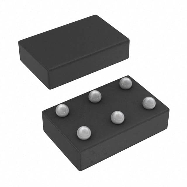
- Package: 8-pin small-outline integrated circuit (SOIC)
- Essence: Provides logic inversion function
- Packaging/Quantity: Available in tape and reel packaging, with 2500 units per reel
Specifications
- Supply Voltage: 1.65V to 5.5V
- Logic Family: LVC (Low-Voltage CMOS)
- Number of Gates: 2
- Propagation Delay: 3.4 ns (typical)
- Operating Temperature Range: -40°C to +85°C
Detailed Pin Configuration
The SN74LVC2G04YZAR has the following pin configuration:
___________
   VCC | 1       8 | GND
   A1  | 2       7 | Y1
   A2  | 3       6 | Y2
   GND | 4       5 | A3
       ‾‾‾‾‾‾‾‾‾‾‾‾‾
Functional Features
- Dual inverter gates: The IC contains two independent inverters.
- High-speed operation: It operates at a fast switching speed, making it suitable for high-frequency applications.
- Low power consumption: The IC is designed to consume minimal power, making it energy-efficient.
- Wide supply voltage range: It can operate within a wide range of supply voltages, providing flexibility in various applications.
Advantages and Disadvantages
Advantages
- Compact size: The small-outline package allows for space-saving integration into electronic circuits.
- Versatile: The logic inversion function can be used in a wide range of digital applications.
- Low power consumption: Ideal for battery-powered devices or energy-efficient designs.
Disadvantages
- Limited number of gates: With only two inverters, it may not be suitable for complex logic circuitry.
- Narrow operating temperature range: It may not be suitable for extreme temperature environments.
Working Principles
The SN74LVC2G04YZAR is based on complementary metal-oxide-semiconductor (CMOS) technology. Each inverter gate consists of a PMOS (p-channel metal-oxide-semiconductor) and NMOS (n-channel metal-oxide-semiconductor) transistor. When the input voltage is high, the PMOS transistor conducts, pulling the output voltage low. Conversely, when the input voltage is low, the NMOS transistor conducts, pulling the output voltage high. This behavior allows for logic inversion.
Detailed Application Field Plans
The SN74LVC2G04YZAR can be used in various digital applications, including:
- Microcontrollers and microprocessors
- Communication systems
- Data transmission and reception
- Signal processing
- Industrial automation
- Consumer electronics
- Automotive electronics
Detailed and Complete Alternative Models
- SN74LVC2G04DCTR: 8-pin surface-mount package with tape and reel packaging.
- SN74LVC2G04DBVR: 6-pin SOT-23 surface-mount package with tape and reel packaging.
- SN74LVC2G04DCKR: 8-pin SC-70 surface-mount package with tape and reel packaging.
- SN74LVC2G04DRLR: 8-pin SON (small-outline no-lead) surface-mount package with tape and reel packaging.
These alternative models offer similar functionality and characteristics to the SN74LVC2G04YZAR, providing options for different package sizes and form factors.
In conclusion, the SN74LVC2G04YZAR is a high-speed, low-power dual inverter gate IC. It offers logic inversion functionality and can be used in various digital applications. Its compact size, versatility, and low power consumption make it a popular choice in the electronics industry.
Lista 10 Vanliga frågor och svar relaterade till tillämpningen av SN74LVC2G04YZAR i tekniska lösningar
Sure! Here are 10 common questions and answers related to the application of SN74LVC2G04YZAR:
Q: What is SN74LVC2G04YZAR? A: SN74LVC2G04YZAR is a dual inverter gate IC (integrated circuit) that can be used for signal inversion or buffering in various technical solutions.
Q: What is the operating voltage range of SN74LVC2G04YZAR? A: The operating voltage range of SN74LVC2G04YZAR is typically between 1.65V and 5.5V.
Q: What is the maximum output current of SN74LVC2G04YZAR? A: The maximum output current of SN74LVC2G04YZAR is typically around 32mA.
Q: Can SN74LVC2G04YZAR be used in battery-powered applications? A: Yes, SN74LVC2G04YZAR can be used in battery-powered applications as it operates at low voltages and has low power consumption.
Q: What is the package type of SN74LVC2G04YZAR? A: SN74LVC2G04YZAR comes in a small SOT-23 package, which is suitable for space-constrained designs.
Q: Is SN74LVC2G04YZAR compatible with both CMOS and TTL logic levels? A: Yes, SN74LVC2G04YZAR is compatible with both CMOS (Complementary Metal-Oxide-Semiconductor) and TTL (Transistor-Transistor Logic) logic levels.
Q: Can SN74LVC2G04YZAR be used for level shifting applications? A: Yes, SN74LVC2G04YZAR can be used for level shifting applications as it supports voltage translation between different logic levels.
Q: What is the propagation delay of SN74LVC2G04YZAR? A: The propagation delay of SN74LVC2G04YZAR is typically around 4.3ns.
Q: Can SN74LVC2G04YZAR drive capacitive loads? A: Yes, SN74LVC2G04YZAR can drive small capacitive loads without requiring additional buffering.
Q: Are there any recommended decoupling capacitors for SN74LVC2G04YZAR? A: It is generally recommended to use a 0.1µF ceramic capacitor placed close to the power supply pins of SN74LVC2G04YZAR for proper decoupling.
Please note that the answers provided here are general and may vary depending on specific application requirements.