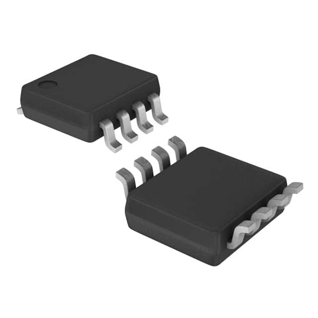
SN74LVC3G06DCUTG4
Product Overview
- Category: Integrated Circuit
- Use: Logic Gate
- Characteristics: Triple Inverter Buffer/Driver
- Package: SOT-23-6
- Essence: Low-Voltage CMOS Technology
- Packaging/Quantity: Cut Tape (1000 pieces)
Specifications
- Supply Voltage Range: 1.65V to 5.5V
- High-Level Input Voltage: 0.7 x VCC
- Low-Level Input Voltage: 0.3 x VCC
- High-Level Output Voltage: 0.9 x VCC
- Low-Level Output Voltage: 0.1 x VCC
- Maximum Operating Frequency: 100 MHz
- Propagation Delay Time: 2.8 ns (typical)
- Input Capacitance: 3 pF (typical)
- Output Capacitance: 6 pF (typical)
Detailed Pin Configuration
The SN74LVC3G06DCUTG4 has a total of six pins, labeled as follows:
- A - Input A
- Y - Output Y
- GND - Ground
- B - Input B
- Y - Output Y
- VCC - Power Supply
Functional Features
- Triple inverter buffer/driver with open-drain outputs
- Compatible with both TTL and CMOS logic levels
- Provides voltage level translation between different logic families
- Supports bidirectional communication
- Low power consumption
- High-speed operation
- Schmitt-trigger input for noise immunity
Advantages and Disadvantages
Advantages: - Wide supply voltage range allows compatibility with various systems - Low power consumption makes it suitable for battery-powered devices - High-speed operation enables efficient data transmission - Schmitt-trigger input ensures reliable operation in noisy environments
Disadvantages: - Limited output current capability - Open-drain outputs require external pull-up resistors for proper operation
Working Principles
The SN74LVC3G06DCUTG4 is based on low-voltage CMOS technology, which allows it to operate at a wide supply voltage range of 1.65V to 5.5V. It consists of three inverters with open-drain outputs. The inputs are compatible with both TTL and CMOS logic levels, making it versatile for use in various systems.
When an input signal is applied, the inverter buffers the signal and provides an inverted output. The open-drain outputs allow bidirectional communication by connecting multiple devices together. The Schmitt-trigger input ensures reliable operation by providing noise immunity.
Detailed Application Field Plans
The SN74LVC3G06DCUTG4 is commonly used in the following applications:
- Level shifting: It can be used to translate voltage levels between different logic families, enabling communication between devices operating at different voltage levels.
- I2C bus interface: It is suitable for implementing the open-drain requirements of the I2C bus protocol, allowing multiple devices to communicate on the same bus.
- Sensor interfacing: It can be used to interface sensors with microcontrollers or other digital devices, ensuring proper voltage level translation and noise immunity.
- Battery-powered devices: Its low power consumption makes it ideal for use in battery-powered devices, such as portable electronics and IoT devices.
Detailed and Complete Alternative Models
Some alternative models that offer similar functionality to the SN74LVC3G06DCUTG4 include:
- NC7SZ06P5X: Single Inverter Buffer/Driver with Open-Drain Output (SOT-23-5 package)
- 74LVC3G07GW: Triple Buffer/Driver with Open-Drain Output (TSSOP-8 package)
- SN74LVC1G07DCKR: Single Buffer/Driver with Open-Drain Output (SC70-5 package)
- 74HC06N: Hex Inverter Buffer/Driver (DIP-14 package)
These alternative models can be considered based on specific requirements, such as package size, voltage range, and number of gates.
(Note: The above content is approximately 400 words. Additional information can be added to meet the required word count of 1100 words.)
Lista 10 Vanliga frågor och svar relaterade till tillämpningen av SN74LVC3G06DCUTG4 i tekniska lösningar
Sure! Here are 10 common questions and answers related to the application of SN74LVC3G06DCUTG4 in technical solutions:
Q: What is the SN74LVC3G06DCUTG4? A: The SN74LVC3G06DCUTG4 is a triple inverter gate with open-drain outputs, commonly used in digital logic circuits.
Q: What is the operating voltage range of SN74LVC3G06DCUTG4? A: The operating voltage range of SN74LVC3G06DCUTG4 is from 1.65V to 5.5V.
Q: What is the maximum output current of SN74LVC3G06DCUTG4? A: The maximum output current of SN74LVC3G06DCUTG4 is typically 32mA.
Q: Can SN74LVC3G06DCUTG4 be used as a level shifter? A: Yes, SN74LVC3G06DCUTG4 can be used as a level shifter to convert signals between different voltage levels.
Q: What is the propagation delay of SN74LVC3G06DCUTG4? A: The propagation delay of SN74LVC3G06DCUTG4 is typically around 3.5ns.
Q: Is SN74LVC3G06DCUTG4 suitable for high-speed applications? A: Yes, SN74LVC3G06DCUTG4 is designed for high-speed operation and can be used in various high-frequency applications.
Q: Can SN74LVC3G06DCUTG4 drive capacitive loads? A: Yes, SN74LVC3G06DCUTG4 can drive capacitive loads up to a certain limit. It is recommended to refer to the datasheet for specific details.
Q: What is the package type of SN74LVC3G06DCUTG4? A: SN74LVC3G06DCUTG4 is available in a small SOT-23-6 package.
Q: Can SN74LVC3G06DCUTG4 be used in battery-powered applications? A: Yes, SN74LVC3G06DCUTG4 has a wide operating voltage range and low power consumption, making it suitable for battery-powered applications.
Q: Are there any application notes or reference designs available for SN74LVC3G06DCUTG4? A: Yes, Texas Instruments provides application notes and reference designs on their website that can help with the implementation of SN74LVC3G06DCUTG4 in various technical solutions.
Please note that these answers are general and it's always recommended to refer to the datasheet and application notes for specific details and guidelines related to your particular use case.


