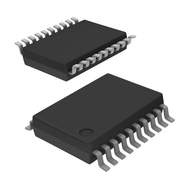
SN74LVC541ADBRG4
Product Overview
- Category: Integrated Circuit (IC)
- Use: Buffer/Driver
- Characteristics: Low Voltage, CMOS Technology
- Package: SSOP (Shrink Small Outline Package)
- Essence: High-Speed, Non-Inverting Buffer/Driver
- Packaging/Quantity: Tape and Reel, 2500 pieces per reel
Specifications
- Supply Voltage: 1.65V to 3.6V
- Input Voltage Levels: VIL = 0.8V, VIH = 2V
- Output Voltage Levels: VOL = 0.1V, VOH = VCC - 0.1V
- Operating Temperature Range: -40°C to +85°C
- Propagation Delay: 3.8ns (typical)
- Output Drive Capability: ±24mA
- Number of Pins: 20
Pin Configuration
The pin configuration of SN74LVC541ADBRG4 is as follows:
__    __
   A1 |1  `--' 20| VCC
   A2 |2        19| OE#
   B1 |3        18| I/O1
   B2 |4        17| I/O2
   B3 |5        16| I/O3
   B4 |6        15| I/O4
   GND|7        14| I/O5
  I/O1|8        13| I/O6
  I/O2|9        12| I/O7
  I/O3|10       11| I/O8
       ``````````
Functional Features
- Non-inverting buffer/driver with 3-state outputs
- High-speed operation suitable for various applications
- Compatible with both TTL and CMOS voltage levels
- Provides output drive capability of ±24mA
- Supports bidirectional data flow
Advantages and Disadvantages
Advantages
- Low power consumption due to CMOS technology
- Wide operating voltage range allows compatibility with different systems
- High-speed operation enables efficient data transfer
- 3-state outputs provide flexibility in controlling data flow
Disadvantages
- Limited number of I/O pins (8 in total)
- Not suitable for high-voltage applications
Working Principles
SN74LVC541ADBRG4 is a non-inverting buffer/driver IC that amplifies and buffers digital signals. It operates using complementary metal-oxide-semiconductor (CMOS) technology, which ensures low power consumption and compatibility with both TTL and CMOS voltage levels.
The IC has 8 input/output (I/O) pins that can be bidirectional, allowing data to flow in both directions. The 3-state outputs provide the ability to disable the outputs, effectively disconnecting them from the circuit.
When the Output Enable (OE#) pin is low, the outputs are enabled and mirror the inputs. Conversely, when OE# is high, the outputs are disabled and enter a high-impedance state.
Detailed Application Field Plans
SN74LVC541ADBRG4 finds applications in various fields where buffering and driving of digital signals are required. Some common application areas include:
- Microcontrollers and microprocessors
- Communication systems
- Data storage devices
- Industrial automation
- Automotive electronics
- Consumer electronics
In microcontroller and microprocessor systems, the IC can be used to interface with external devices such as memory modules, displays, or communication peripherals.
Communication systems benefit from SN74LVC541ADBRG4's high-speed operation, allowing efficient data transfer between different components.
Data storage devices, such as hard drives or solid-state drives, utilize the IC to amplify and buffer signals during read/write operations.
Industrial automation systems often require buffering and driving of control signals, making SN74LVC541ADBRG4 suitable for various applications in this field.
Automotive electronics rely on robust and reliable signal buffering, and the IC meets these requirements, making it suitable for automotive applications.
Consumer electronics, including smartphones, tablets, and gaming consoles, can benefit from the IC's low power consumption and high-speed operation.
Detailed and Complete Alternative Models
- SN74LVC244A: Octal Buffer/Driver with 3-State Outputs
- SN74LVC125A: Quad Buffer/Driver with 3-State Outputs
- SN74LVC07A: Hex Buffer/Driver with Open-Drain Outputs
- SN74LVC1G07: Single Buffer/Driver with Open-Drain Output
- SN74LVC2G07: Dual Buffer/Driver with Open-Drain Outputs
Lista 10 Vanliga frågor och svar relaterade till tillämpningen av SN74LVC541ADBRG4 i tekniska lösningar
Sure! Here are 10 common questions and answers related to the application of SN74LVC541ADBRG4:
Q: What is SN74LVC541ADBRG4? A: SN74LVC541ADBRG4 is a type of octal buffer/line driver with 3-state outputs, commonly used in digital systems.
Q: What is the voltage supply range for SN74LVC541ADBRG4? A: The voltage supply range for SN74LVC541ADBRG4 is typically between 1.65V and 5.5V.
Q: What is the maximum output current of SN74LVC541ADBRG4? A: The maximum output current of SN74LVC541ADBRG4 is typically around 32mA.
Q: Can SN74LVC541ADBRG4 be used as a level shifter? A: Yes, SN74LVC541ADBRG4 can be used as a level shifter to convert signals between different voltage levels.
Q: How many input/output pins does SN74LVC541ADBRG4 have? A: SN74LVC541ADBRG4 has 8 input pins and 8 output pins.
Q: What is the purpose of the 3-state outputs in SN74LVC541ADBRG4? A: The 3-state outputs allow the device to be effectively disconnected from the bus, enabling multiple devices to share the same bus without interference.
Q: Can SN74LVC541ADBRG4 handle high-speed data transmission? A: Yes, SN74LVC541ADBRG4 is designed to handle high-speed data transmission, making it suitable for applications with fast data rates.
Q: What is the maximum operating frequency of SN74LVC541ADBRG4? A: The maximum operating frequency of SN74LVC541ADBRG4 is typically around 100MHz.
Q: Can SN74LVC541ADBRG4 be used in both digital and analog circuits? A: No, SN74LVC541ADBRG4 is specifically designed for digital circuits and should not be used in analog applications.
Q: Are there any specific precautions to consider when using SN74LVC541ADBRG4? A: It is important to ensure that the voltage supply range and input/output voltage levels are within the specified limits. Additionally, proper decoupling capacitors should be used to minimize noise and ensure stable operation.
Please note that these answers are general and may vary depending on the specific application and requirements.


