

SN74LVC541ADGVRE4
Overview
Category: Integrated Circuit (IC)
Use: The SN74LVC541ADGVRE4 is a high-performance octal buffer and line driver designed for 3.3V systems. It is commonly used to provide buffering and signal amplification in digital circuits.
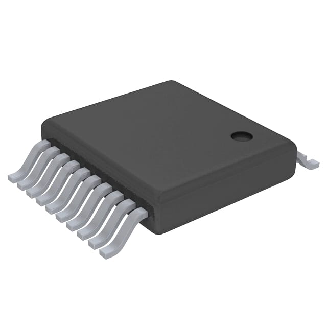
Characteristics: - Operating Voltage: 3.3V - Number of Channels: 8 - Output Current: ±24mA - Input Voltage Range: 0V to VCC - Package Type: TSSOP - Package Quantity: 56 pieces per reel
Essence: The SN74LVC541ADGVRE4 is an essential component in electronic devices that require reliable signal transmission and amplification. Its high-performance characteristics make it suitable for various applications.
Specifications
The specifications of the SN74LVC541ADGVRE4 are as follows:
- Supply Voltage Range: 1.65V to 3.6V
- High-Level Input Voltage: 2V to VCC + 0.5V
- Low-Level Input Voltage: -0.5V to 0.8V
- High-Level Output Voltage: VCC - 0.5V
- Low-Level Output Voltage: 0.5V
- Maximum Propagation Delay: 4.3ns
- Maximum Operating Frequency: 100MHz
Pin Configuration
The detailed pin configuration of the SN74LVC541ADGVRE4 is as follows:
__    __
   A1 | 1    56 | VCC
   A2 | 2    55 | OE#
   B1 | 3    54 | I/O1
   B2 | 4    53 | GND
   C1 | 5    52 | I/O2
   C2 | 6    51 | GND
   D1 | 7    50 | I/O3
   D2 | 8    49 | GND
   E1 | 9    48 | I/O4
   E2 |10    47 | GND
   F1 |11    46 | I/O5
   F2 |12    45 | GND
   G1 |13    44 | I/O6
   G2 |14    43 | GND
   H1 |15    42 | I/O7
   H2 |16    41 | GND
 GND |17    40 | I/O8
  VCC |18    39 | DIR#
  I/O1|19    38 | A1
   OE#|20    37 | A2
  I/O2|21    36 | B1
  GND |22    35 | B2
  I/O3|23    34 | C1
  GND |24    33 | C2
  I/O4|25    32 | D1
  GND |26    31 | D2
  I/O5|27    30 | E1
  GND |28    29 | E2
       ‾‾    ‾‾
Functional Features
The SN74LVC541ADGVRE4 offers the following functional features:
- Octal buffer and line driver with 3-state outputs
- Non-inverting outputs
- High-speed operation
- Low static power consumption
- Supports mixed-mode signal operation on all ports
- Overvoltage-tolerant inputs
- Inputs and outputs are 5V tolerant
- ESD protection exceeds 2000V HBM per JESD22-A114 and 1000V CDM per JESD22-C101
Advantages and Disadvantages
Advantages: - High-performance buffer and line driver - Wide operating voltage range - Low power consumption - Overvoltage protection - 5V tolerant inputs and outputs - ESD protection
Disadvantages: - Limited to 8 channels - Not suitable for high-frequency applications above 100MHz
Working Principles
The SN74LVC541ADGVRE4 operates by receiving input signals on its eight channels and amplifying them to provide higher current drive capability. The non-inverting outputs allow the signal to be transmitted without phase inversion. The 3-state outputs enable the device to be effectively disconnected from the bus when not in use.
Application Field Plans
The SN74LVC541ADGVRE4 is widely used in various applications, including but not limited to:
- Microprocessor-based systems
- Data communication systems
- Industrial control systems
- Automotive electronics
Lista 10 Vanliga frågor och svar relaterade till tillämpningen av SN74LVC541ADGVRE4 i tekniska lösningar
Sure! Here are 10 common questions and answers related to the application of SN74LVC541ADGVRE4:
Q: What is SN74LVC541ADGVRE4? A: SN74LVC541ADGVRE4 is a non-inverting octal buffer and line driver with 3-state outputs, commonly used in digital systems.
Q: What is the operating voltage range for SN74LVC541ADGVRE4? A: The operating voltage range for SN74LVC541ADGVRE4 is from 1.65V to 5.5V.
Q: What is the maximum output current that SN74LVC541ADGVRE4 can drive? A: SN74LVC541ADGVRE4 can drive up to 32mA of output current per channel.
Q: Can SN74LVC541ADGVRE4 be used as a level shifter? A: Yes, SN74LVC541ADGVRE4 can be used as a level shifter to convert signals between different voltage levels.
Q: How many input/output channels does SN74LVC541ADGVRE4 have? A: SN74LVC541ADGVRE4 has 8 input/output channels.
Q: What is the typical propagation delay of SN74LVC541ADGVRE4? A: The typical propagation delay of SN74LVC541ADGVRE4 is around 3.9ns.
Q: Can SN74LVC541ADGVRE4 be used in high-speed applications? A: Yes, SN74LVC541ADGVRE4 is designed for high-speed operation and can be used in such applications.
Q: Does SN74LVC541ADGVRE4 have built-in ESD protection? A: Yes, SN74LVC541ADGVRE4 has built-in ESD protection to safeguard against electrostatic discharge.
Q: Can SN74LVC541ADGVRE4 be used in both parallel and serial communication systems? A: Yes, SN74LVC541ADGVRE4 can be used in both parallel and serial communication systems as a buffer or line driver.
Q: Is SN74LVC541ADGVRE4 available in different package options? A: Yes, SN74LVC541ADGVRE4 is available in various package options, including SOIC, TSSOP, and VQFN.
Please note that these answers are general and may vary depending on the specific application and requirements. It's always recommended to refer to the datasheet and consult with technical experts for accurate information.