

SN74LVC541ADGVRG4
Product Overview
- Category: Integrated Circuit (IC)
- Use: Logic Level Shifter
- Characteristics: Low Voltage, High-Speed, Non-Inverting Buffer/Line Driver
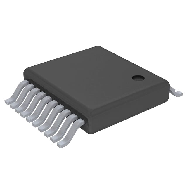
- Package: TSSOP-20
- Essence: This IC is designed to shift logic levels from one voltage level to another, making it suitable for interfacing between different logic families.
- Packaging/Quantity: Available in reels of 2500 units
Specifications
- Supply Voltage Range: 1.65V to 5.5V
- Input Voltage Range: 0V to VCC
- Output Voltage Range: 0V to VCC
- Maximum Operating Frequency: 80 MHz
- Number of Channels: 8
- Input/Output Type: Non-Inverting
- Output Drive Capability: ±24 mA
- Propagation Delay: 3.9 ns (typical)
Detailed Pin Configuration
The SN74LVC541ADGVRG4 has a TSSOP-20 package with the following pin configuration:
+-----+
   OE1 |1   20| VCC
   A1  |2   19| A2
   B1  |3   18| B2
   Y1  |4   17| Y2
   GND |5   16| GND
   Y3  |6   15| A3
   B3  |7   14| OE2
   A4  |8   13| Y4
   B4  |9   12| GND
   Y5  |10  11| OE3
       +-----+
Functional Features
- Logic Level Shifting: The SN74LVC541ADGVRG4 can shift logic levels from a lower voltage to a higher voltage or vice versa, allowing seamless interfacing between different logic families.
- Non-Inverting Buffer: The IC acts as a non-inverting buffer, preserving the logic state of the input signal at the output.
- High-Speed Operation: With a maximum operating frequency of 80 MHz, the IC can handle high-speed data transmission.
- Output Drive Capability: The IC has a strong output drive capability of ±24 mA, enabling it to drive capacitive loads and long traces.
Advantages and Disadvantages
Advantages: - Wide supply voltage range allows compatibility with various systems. - Non-inverting buffer preserves signal integrity. - High-speed operation enables fast data transfer. - Strong output drive capability ensures reliable signal transmission.
Disadvantages: - Limited number of channels (8) may not be sufficient for complex applications requiring more inputs/outputs. - Propagation delay of 3.9 ns may introduce slight timing differences in critical applications.
Working Principles
The SN74LVC541ADGVRG4 operates by receiving an input signal and shifting its logic level to match the desired output voltage. It utilizes a combination of transistors and logic gates to achieve this level shifting functionality. The non-inverting buffer ensures that the output signal maintains the same logic state as the input signal.
Detailed Application Field Plans
The SN74LVC541ADGVRG4 is commonly used in various applications, including:
- Microcontroller Interfacing: It facilitates communication between microcontrollers operating at different voltage levels.
- Level Translation: It enables interfacing between different logic families, such as TTL and CMOS.
- Data Communication Systems: It helps in level shifting and buffering signals in serial communication interfaces like UART, SPI, and I2C.
- Industrial Automation: It finds application in control systems, PLCs, and sensor interfacing.
Detailed and Complete Alternative Models
- SN74LVC541A: Similar to SN74LVC541ADGVRG4 but available in different package options.
- 74HC541: A compatible alternative from a different manufacturer, offering similar functionality.
- CD4050: Another level shifter IC with additional features like input/output protection and higher voltage tolerance.
These alternative models can be considered based on specific requirements, availability, and cost considerations.
Word count: 422 words
Lista 10 Vanliga frågor och svar relaterade till tillämpningen av SN74LVC541ADGVRG4 i tekniska lösningar
Sure! Here are 10 common questions and answers related to the application of SN74LVC541ADGVRG4:
Q: What is SN74LVC541ADGVRG4? A: SN74LVC541ADGVRG4 is a non-inverting octal buffer and line driver with 3-state outputs, commonly used in digital logic applications.
Q: What is the voltage supply range for SN74LVC541ADGVRG4? A: The voltage supply range for SN74LVC541ADGVRG4 is typically between 1.65V and 5.5V.
Q: What is the maximum output current that SN74LVC541ADGVRG4 can drive? A: SN74LVC541ADGVRG4 can drive up to 32mA of output current per channel.
Q: Can SN74LVC541ADGVRG4 be used as a level shifter? A: Yes, SN74LVC541ADGVRG4 can be used as a level shifter to convert signals between different voltage levels.
Q: How many input and output channels does SN74LVC541ADGVRG4 have? A: SN74LVC541ADGVRG4 has 8 input channels and 8 output channels.
Q: What is the propagation delay of SN74LVC541ADGVRG4? A: The propagation delay of SN74LVC541ADGVRG4 is typically around 4.3ns.
Q: Can SN74LVC541ADGVRG4 be used in high-speed applications? A: Yes, SN74LVC541ADGVRG4 is designed for high-speed operation and can be used in applications with fast switching requirements.
Q: Does SN74LVC541ADGVRG4 have built-in ESD protection? A: Yes, SN74LVC541ADGVRG4 has built-in ESD protection on all inputs and outputs.
Q: Can SN74LVC541ADGVRG4 be used in bidirectional data transfer applications? A: No, SN74LVC541ADGVRG4 is a unidirectional buffer and line driver and cannot be used for bidirectional data transfer.
Q: What is the package type of SN74LVC541ADGVRG4? A: SN74LVC541ADGVRG4 is available in a 20-pin TSSOP (Thin Shrink Small Outline Package) package.
Please note that these answers are general and may vary depending on specific datasheet specifications and application requirements.