

TLC5510INS
Product Overview
- Category: Integrated Circuit (IC)
- Use: Analog-to-Digital Converter (ADC)
- Characteristics: High-resolution, low-power consumption
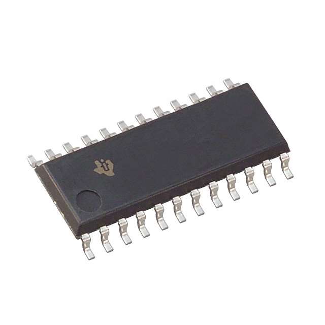
- Package: DIP-16 (Dual In-line Package with 16 pins)
- Essence: Converts analog signals into digital data
- Packaging/Quantity: Available in reels of 250 units
Specifications
- Resolution: 10 bits
- Sampling Rate: 100 kilosamples per second (ksps)
- Input Voltage Range: 0 to 5 volts
- Power Supply Voltage: 2.7 to 5.5 volts
- Operating Temperature Range: -40°C to +85°C
Pin Configuration
The TLC5510INS has a total of 16 pins, which are assigned as follows:
- VREFH: Reference voltage high
- VREFL: Reference voltage low
- AGND: Analog ground
- VIN: Analog input
- CLK: Clock input
- CS: Chip select input
- DOUT: Digital output
- DGND: Digital ground
- DB11: Data bit 11
- DB10: Data bit 10
- DB9: Data bit 9
- DB8: Data bit 8
- DB7: Data bit 7
- DB6: Data bit 6
- DB5: Data bit 5
- DB4: Data bit 4
Functional Features
- High-resolution conversion of analog signals to digital data
- Low power consumption for energy-efficient operation
- Wide input voltage range allows for versatile applications
- Fast sampling rate enables real-time data acquisition
- Serial interface for easy integration with microcontrollers
Advantages and Disadvantages
Advantages
- High accuracy in converting analog signals
- Low power consumption extends battery life
- Compact package for space-constrained designs
- Easy integration with microcontrollers
- Wide operating temperature range for various environments
Disadvantages
- Limited resolution compared to higher-end ADCs
- Requires an external clock source for operation
- Not suitable for applications requiring higher sampling rates
Working Principles
The TLC5510INS is based on the successive approximation technique for analog-to-digital conversion. It utilizes a built-in reference voltage and compares the input analog signal against a series of binary-weighted voltages. By iteratively adjusting the digital code, the converter determines the closest digital representation of the input signal.
Detailed Application Field Plans
The TLC5510INS is commonly used in various applications, including:
- Industrial automation systems
- Data acquisition systems
- Medical equipment
- Instrumentation and measurement devices
- Audio processing equipment
Alternative Models
For alternative options, consider the following ADCs:
- ADC0804: 8-bit resolution, lower cost
- ADS1115: 16-bit resolution, higher accuracy
- MCP3208: 12-bit resolution, SPI interface
These alternatives provide different resolutions, interfaces, and features to suit specific application requirements.
In conclusion, the TLC5510INS is a high-resolution, low-power analog-to-digital converter. With its compact package and versatile characteristics, it finds applications in various fields such as industrial automation, data acquisition, and medical equipment. While it may have limitations in terms of resolution and sampling rate, alternative models offer different specifications to cater to diverse needs.
Lista 10 Vanliga frågor och svar relaterade till tillämpningen av TLC5510INS i tekniska lösningar
Sure! Here are 10 common questions and answers related to the application of TLC5510INS in technical solutions:
Q: What is TLC5510INS? A: TLC5510INS is a high-resolution, 8-channel, 10-bit analog-to-digital converter (ADC) designed for various technical applications.
Q: What is the operating voltage range of TLC5510INS? A: The operating voltage range of TLC5510INS is typically between 2.7V and 5.5V.
Q: How many analog input channels does TLC5510INS have? A: TLC5510INS has 8 analog input channels, allowing simultaneous conversion of multiple signals.
Q: What is the maximum sampling rate of TLC5510INS? A: The maximum sampling rate of TLC5510INS is typically 200 kilosamples per second (ksps).
Q: Can TLC5510INS operate in both single-ended and differential mode? A: Yes, TLC5510INS can be configured to operate in either single-ended or differential mode, depending on the application requirements.
Q: Does TLC5510INS have an internal reference voltage? A: No, TLC5510INS does not have an internal reference voltage. An external reference voltage must be provided for accurate conversions.
Q: What is the resolution of TLC5510INS? A: TLC5510INS has a resolution of 10 bits, providing 1024 possible output values.
Q: Is TLC5510INS suitable for low-power applications? A: Yes, TLC5510INS is designed for low-power operation, making it suitable for battery-powered or energy-efficient devices.
Q: Can TLC5510INS interface with microcontrollers or digital systems? A: Yes, TLC5510INS has a serial interface (SPI) that allows easy integration with microcontrollers and other digital systems.
Q: What are some typical applications of TLC5510INS? A: TLC5510INS can be used in various applications such as data acquisition systems, industrial automation, medical devices, instrumentation, and sensor interfaces.
Please note that the answers provided here are general and may vary depending on specific datasheet specifications and application requirements.