

TLV2783CDGSRG4
Product Overview
- Category: Integrated Circuit (IC)
- Use: Operational Amplifier
- Characteristics: Low-voltage, Rail-to-Rail Input/Output, General Purpose
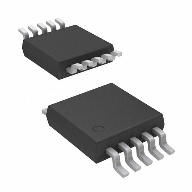
- Package: VSSOP-8
- Essence: TLV2783CDGSRG4 is a low-voltage operational amplifier designed for general-purpose applications. It offers rail-to-rail input and output capabilities, making it suitable for various voltage levels.
- Packaging/Quantity: The TLV2783CDGSRG4 is available in a VSSOP-8 package and is typically sold in reels of 2500 units.
Specifications
- Supply Voltage: 2.7V to 5.5V
- Input Offset Voltage: ±1mV (maximum)
- Input Bias Current: ±1pA (maximum)
- Gain Bandwidth Product: 10MHz
- Slew Rate: 6V/µs
- Operating Temperature Range: -40°C to +125°C
Detailed Pin Configuration
The TLV2783CDGSRG4 has the following pin configuration:
___________
  OUT | 1       6 | VCC+
  IN- | 2       5 | IN+
  IN+ | 3       4 | GND
       ‾‾‾‾‾‾‾‾‾‾‾
Functional Features
- Low-voltage operation allows for compatibility with battery-powered devices.
- Rail-to-rail input/output capability enables accurate signal amplification across the entire supply voltage range.
- General-purpose design makes it suitable for a wide range of applications.
- High gain bandwidth product and slew rate ensure fast and accurate signal processing.
Advantages and Disadvantages
Advantages: - Low-voltage operation extends battery life in portable devices. - Rail-to-rail input/output capability provides accurate signal amplification. - General-purpose design allows for versatile use in various applications. - High gain bandwidth product and slew rate enable fast and precise signal processing.
Disadvantages: - Limited number of channels (3) compared to multi-channel operational amplifiers. - Relatively small package size may require careful handling during assembly.
Working Principles
The TLV2783CDGSRG4 is an operational amplifier that amplifies the difference between its two input voltages. It operates on a low-voltage supply, typically ranging from 2.7V to 5.5V. The rail-to-rail input/output capability ensures that the amplifier can accurately amplify signals even when they approach the supply voltage limits.
The amplifier's internal circuitry consists of transistors and resistors that work together to provide high gain and low distortion. The input stage amplifies the voltage difference between the IN+ and IN- pins, while the output stage drives the amplified signal to the OUT pin.
Detailed Application Field Plans
The TLV2783CDGSRG4 is commonly used in various applications, including:
- Portable Devices: Due to its low-voltage operation and rail-to-rail capabilities, it is suitable for battery-powered devices such as smartphones, tablets, and portable audio players.
- Sensor Interfaces: The amplifier can be used to interface with sensors that produce low-level signals, such as temperature sensors, pressure sensors, and light sensors.
- Signal Conditioning: It can be employed in signal conditioning circuits to amplify weak signals before further processing or transmission.
- Audio Amplification: The TLV2783CDGSRG4 can be utilized in audio amplifiers, headphone amplifiers, and audio mixers to enhance audio signals.
Detailed and Complete Alternative Models
- LM324: A quad operational amplifier with similar characteristics, but with four independent channels.
- MCP6004: A quad operational amplifier with rail-to-rail input/output capability and low power consumption.
- AD8628: A precision operational amplifier with low offset voltage and low noise performance.
These alternative models offer similar functionality and can be considered as substitutes for the TLV2783CDGSRG4 in various applications.
Word count: 520 words
Lista 10 Vanliga frågor och svar relaterade till tillämpningen av TLV2783CDGSRG4 i tekniska lösningar
Sure! Here are 10 common questions and answers related to the application of TLV2783CDGSRG4 in technical solutions:
Q: What is TLV2783CDGSRG4? A: TLV2783CDGSRG4 is a low-power, rail-to-rail input/output operational amplifier (op-amp) that is commonly used in various electronic applications.
Q: What is the supply voltage range for TLV2783CDGSRG4? A: The supply voltage range for TLV2783CDGSRG4 is typically between 2.7V and 5.5V.
Q: What is the maximum output current of TLV2783CDGSRG4? A: The maximum output current of TLV2783CDGSRG4 is typically around 20mA.
Q: Can TLV2783CDGSRG4 operate in single-supply mode? A: Yes, TLV2783CDGSRG4 can operate in both single-supply and dual-supply modes.
Q: What is the input offset voltage of TLV2783CDGSRG4? A: The input offset voltage of TLV2783CDGSRG4 is typically around 1mV.
Q: Is TLV2783CDGSRG4 suitable for low-power applications? A: Yes, TLV2783CDGSRG4 is designed for low-power applications, making it ideal for battery-powered devices.
Q: Can TLV2783CDGSRG4 be used in precision measurement circuits? A: Yes, TLV2783CDGSRG4 has low input offset voltage and low noise characteristics, making it suitable for precision measurement circuits.
Q: What is the bandwidth of TLV2783CDGSRG4? A: The bandwidth of TLV2783CDGSRG4 is typically around 10MHz.
Q: Does TLV2783CDGSRG4 have built-in ESD protection? A: Yes, TLV2783CDGSRG4 has built-in electrostatic discharge (ESD) protection to safeguard against damage during handling and assembly.
Q: Can TLV2783CDGSRG4 be used in automotive applications? A: Yes, TLV2783CDGSRG4 is qualified for automotive applications and meets the necessary standards for reliability and performance.
Please note that the answers provided here are general and may vary depending on specific datasheet specifications and application requirements.